The performance of communication systems depends on the speed of the devices used, and is typically specified by two figures-of-merit (FOM). The first FOM is the transistor cut-off frequency fT; the second FOM is the maximum oscillation frequency fmax (defined as the frequency at which the current gain and the power gain become unity, respectively).
To meet this challenge, the transistor geometric profile needs to be scaled for higher fT and fmax. Technology scaling has driven this momentum to a high level of integration.1 Device scaling has been the critical driving force behind high speed integrated RF (radio frequency) and MW (microwave) solutions. Since the operating frequency of the oscillator is limited by the fT of the transistors, RF and MW integrated circuits are often designed using GaAs HBTs, which offer high fT, but typically exhibit higher flicker corner frequency (fc) and are power hungry, and are therefore not suitable for low phase noise and power efficiency in signal generation applications.1–19 Si BJTs typically have a low flicker corner frequency, but do not have sufficient gain to sustain stable oscillation at RF and microwave frequencies because of their limited fT and fmax.14 SiGe HBTs offer lower fc and comparable fT to GaAs HBTs, making them the favorable choice for low phase noise and power-efficient RF and MW signal generation applications.13,14 The oscillator phase noise performance is one of the areas where SiGe HBT devices outperform III-V devices.16,17 SiGe HBT has progressed over the last decade from a digitally oriented technology to one well suited for RF and microwave applications (due to its superior analog and RF performance and its CMOS integration capability).13–19 Hence, SiGe HBT technology is a promising contender among Si-based technology, due to its advantages over CMOS technology such as higher fT, lower noise and power-efficient performance. This article discusses the impact of scaling on phase noise and the minimization of phase noise in SiGe HBTs coupled voltage-controlled oscillators (VCO).
Scaling and noise performance characteristics
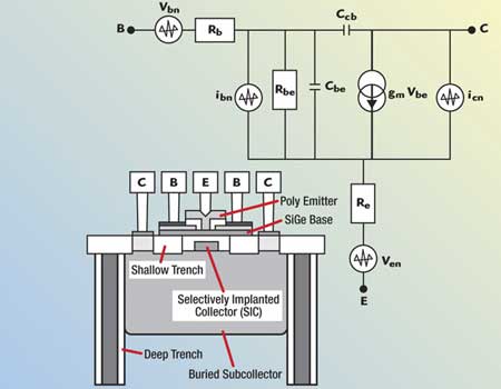
Fig. 1 CE equivalent circuit noise model of the SiGe HBT transistor.
Figure 1 shows the typical simplified common emitter equivalent circuit broadband noise model of the SiGe HBT transistor.17 The fT and fmax of SiGe HBT can be given by
where
Cbe = parasitic emitter base junction capacitance
Ccb = parasitic collector base junction capacitance
Rb = parasitic base resistance
gm = device transconductance
τb = base transit time
τe = emitter delay time
τbc = base collector junction depletion layer time
All are technological scaling sensitive device parameters and can be optimized for higher fT and minimum noise figure for high frequency low noise oscillator applications.
Active devices (bipolar transistor) contribute their own set of problems for the oscillator designer due to their inherent nonlinearities, noise properties and temperature variations. The designer has limited control over the noise sources in transistor, and only has a choice of device selection, oscillator topology and operating bias point. For better insight into the noise effects in the oscillator design, it is necessary to understand how the noise arises in transistor and oscillator circuits. Noise in the active device is characterized as a broadband noise (base and collector current shot noise, and base resistance thermal noise) and low frequency noise (1/f noise), which are sensitive to the scaling of the active device3
Broadband noise (thermal and shot noise)
The broadband noise in a bipolar transistor is due to the base current shot noise 2qIB, the collector current shot noise 2qIC, the base resistance thermal noise 4kTRb and the emitter resistance thermal noise 4kTRe. The mean square values of the broadband noise generator (scaling sensitive parameters), as shown in the figure for a frequency interval Δf, can be described by
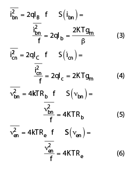
From Equations 1 to 4, the base and collector current shot noise can be reduced by increasing the current gain b and cut-off frequency fT for a given profile of a SiGe HBT technology. Increasing the doping profile of the base and reducing the emitter width can minimize the thermal noise generated due to the base resistance.1 From Equations 1 to 6, maximizing the current gain β, the cutoff frequency fT, and lowering the base resistance RB in SiGe HBT, make the technology promising for low phase noise signal sources (oscillator/VCOs).13–19
Low Frequency Noise (1/f Noise: Flicker Noise)
The major contribution of low frequency noise is due to the flicker noise (1/f noise), which lies in the base current of the SiGe HBTs.17 For a spectral pure signal source, a lower 1/f noise is desired to minimize the phase noise. However, the reduction of 1/f noise in semiconductor technology is challenging, because it is sensitive to defects, particularly in scaled technologies with low thermal cycles.1 The origins of 1/f noise are varied, but in bipolar devices, traps associated with contamination and crystal defects in the emitter-base depletion layer cause 1/f noise. These traps capture and release carriers in a random fashion and the time constants associated with the process give rise to a scaling sensitive noise signal that describes a spectral density of the form17
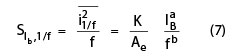
Δf = narrow frequency bandwidth at frequency f
IB = base current
K = constant for a particular device and technology
Ae = emitter area
a = flicker noise exponent (≅2 for SiGe HBTs)
b = flicker noise frequency shaping factor whose value is approximately unity
The mechanism for up-conversion of 1/f noise is caused by the nonlinear nature of the circuits. The 1/f noise plays an important role in determining the close-in carrier phase noise, which is unconverted to the carrier frequency, resulting in a 1/f3 region near the carrier frequency. The SiGe HBTs transistors exhibit typically a 3 to 4 times lower 1/f noise, compared to Si devices.16
Oscillator Phase Noise  and
Noise Factor F
and
Noise Factor F
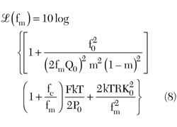
The oscillator phase noise can be given by3
where
m = ratio of the loaded to unloaded Q
Q0 = unloaded Q
QL = loaded Q
f0 = oscillation frequency
fc = flicker corner frequency
fm = offset frequency from the carrier
F = noise factor
K0 = oscillator voltage gain
R = noise resistance of the tuning diode
k = Boltzman’s constant
T = temperature in degree K
From Equation 8, the minimum phase noise can be obtained by minimizing the noise factor F for a given oscillator topology, operating frequency and tuning range. The minimum noise factor Fmin, for the circuit shown, can be described by13–19
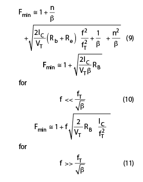
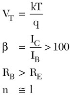
where
From Equation 10, Fmin at low frequency can be minimized by increasing the value of the current gain β and reducing the values of RB at a given device bias (IC = IDC1) condition. However, Fmin at low frequencies can be improved by increasing β, but is limited by the negative impact on the breakdown voltage BVCEO. From Equation 11, at high frequencies, Fmin can be minimized by decreasing the value of RB and increasing fT at a given device bias (IC = IDC2). In SiGe HBTs, the parasitic emitter base junction capacitance Cbe and the parasitic base resistance Rb vary linearly with emitter width we, allowing Fmin at low and high frequency regions to continue scaling down linearly with we. The parasitic emitter base junction capacitance Cbe and the parasitic base resistance Rb decrease proportionally to the emitter strip length Le, whereas Cbe and Rb increase proportionally to the emitter width we. The noise factor F is a technological scaling sensitive parameter and can be optimized with respect to the transistor geometric profile of the scaled SiGe HBTs to obtain the minimum noise figure for low phase noise oscillator applications.
Scaled Device Multi-coupled Resonator VCO (2 to 6 GHz)
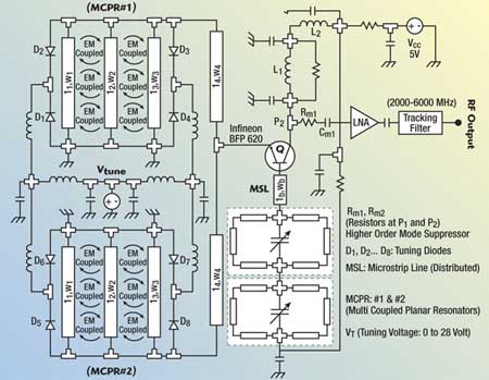
Fig. 2 Schematic of the 2 to 6 GHz coupled resonator VCO (patent pending).
For high frequency applications, vertical scaling is done by reducing the base and collector transit times of the SiGe HBT technology, which requires a narrow and heavily doped base profile, with a higher Ge mole fraction.
Therefore, it results in a lower thermal budget, and an increase in 1/f noise.1 Figures 2 and 3 illustrate the schematic and layout of the multi-coupled resonator-based VCO for a 2 to 6 GHz frequency band (patent pending).
Figure 4 shows the measured phase noise for scaling factors 1:1 and 1:2. As depicted, the device scaling increases the contribution from 1/f noise (near the carrier), whereas it decreases the contribution from base current shot noise and base resistance thermal noise (far from the carrier).
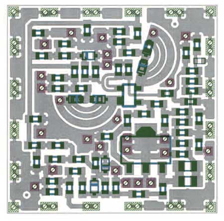
Fig. 3 Layout of the 2 to 6 GHz coupled resonator VCO (patent pending).
As shown, the degradation at 1 kHz offset from the carrier frequency is 3 to 6 dB, whereas the improvement at a 1 MHz offset frequency is 6 to 12 dB.
Therefore, by analyzing the noise behaviors at near and far carrier frequency offsets, due to the device scaling, the designer can improve the noise performance by optimizing the conduction angle for a given size of the device.2–5
The VCO design approach based on scaling demonstrated in this work enables power-efficient (5 V, 20 mA), extended frequency operation, lower phase noise performance with a minimum 5 dBm power output over the band (2 to 6 GHz), which is attractive for present and future generations of wireless applications.5
Coupled Mode Oscillators (N-push)
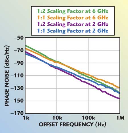
Fig. 4 Measured phase noise plot of a 2 to 6 GHz VCO for scaling 1:1 and 1:2.
A high frequency oscillator signal can be generated, based on either a scaled device (higher cut-off frequency fT) operating at a fundamental frequency or using a multiplier (frequency doubler).2–10 A typical oscillator operating at the fundamental frequency suffers from a low Q factor, insufficient device gain, lower device breakdown voltage and higher phase noise at a high frequency of operation.3
The frequency doubler and other means of up-conversion may provide a practical and quick solution to generate high frequency signal from oscillators operating at a lower frequency, but it introduces distortions and has poor phase noise performances.1–24
This limitation has made it more attractive to pursue alternative approaches such as N-Push VCOs, RF-MEMS (radio frequency micro electromechanical system) VCOs, OEO (opto-electronic oscillator), YIG (yttrium-iron-garnet) VCOs and others.18–21 Recently, an approach based on a coupled oscillator principle in an N-Push (N = 2, 3, 4…k) configuration has brought much attention because this principle allows for an extended operating frequency range of active devices.7
The coupled oscillator N-Push approach improves the phase noise performance by a factor of N (N is the number of the oscillators sub-circuits), and extends the operating frequency beyond the limitation caused by the cut-off frequency of available active devices.
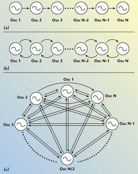
Fig. 5 Systems of N-push oscillators: (a) nearest neighbor unilateral coupling; (b) nearest neighbor bilateral coupling; and (c) global coupling.
Figure 5 shows the system of N-coupled oscillators coupled through the arbitrary coupling network as unilateral coupling, bilateral coupling and global coupling.3 The coupled oscillators approach discussed in this work minimizes the phase noise and extends the operating frequency.5 The drawback of coupled oscillator (N-Push) topology is the presence of higher order nth harmonic components, which may introduce significant 1/f noise up-conversion due to the asymmetrical output waveform in the subsequent N oscillator sub-circuits that forms the N-Push configuration. The expression for the oscillator phase noise can be given by6
where
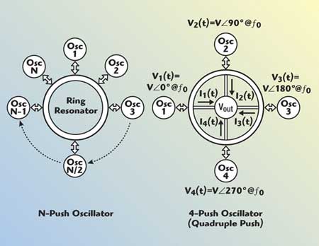
Fig. 6 N-coupled mode oscillators.
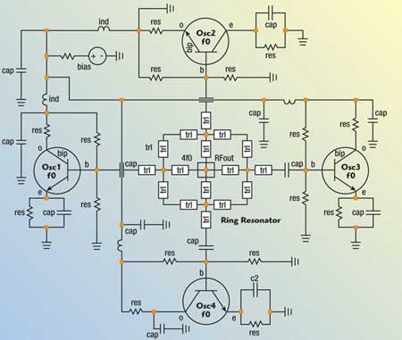
Fig. 7 Schematic of an N-push (N=4) coupled oscillator.
From Equation 15, the 1/f noise up-conversion is closely related to the symmetry property of the oscillator signal waveforms, and the 1/f noise up-conversion can be reduced by minimizing the value of C0 and by optimizing the slope and symmetry of the rise and fall time of the oscillator output waveform.
The phase noise of the N-coupled oscillator in terms of a single uncoupled oscillator can be described by8
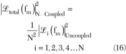
From Equation 16, the N-coupled oscillator system improves the phase noise, compared to the single individual uncoupled oscillator, by a factor N, where N is the number of the uncoupled oscillators in the coupled N-Push topology.5–8
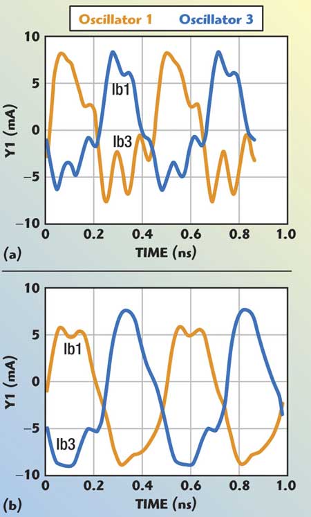
Fig. 8 Simulated RF output current waveforms of the 4-push VCO; (a) asymmetrical and (b) symmetrical.
Scaled Device Coupled Mode 4-Push Oscillators
Figure 6 shows typical simplified N-coupled oscillators, coupled through a common resonator and an example of a 4-Push oscillator. Figure 7 shows the schematic of the 4-Push coupled oscillators operating at a fixed frequency of 8 GHz (4f0).
Figure 8 depicts the simulated plot of the symmetrical and asymmetrical output waveforms for the N-Push (N = 4) VCO, using scaled SiGe HBTs (Infineon BFP620, scaling 1:2). For better insight about the coupled mode N-Push domain, it is necessary to know how the noise is affected by the scaling and symmetry of the waveforms.
From Equations 15 and 16, the noise performance and 1/f noise up-conversion can be optimized by improving the symmetry of the waveform in N-Push topology for a given size of the device.
Figure 9 shows the improvement in phase noise performance for a scaled coupled mode 4-Push VCO. At 1 kHz offset, it is of the order of 6 to 10 dB, whereas at 1 MHz offset the improvement is of the order of 8 to 15 dB for a device area scaling factor of 1:2.
Figures 10 and 11 show the block diagram and layout of the scaled device coupled mode multi-octave band 2-Push VCO (2 to 8 GHz).
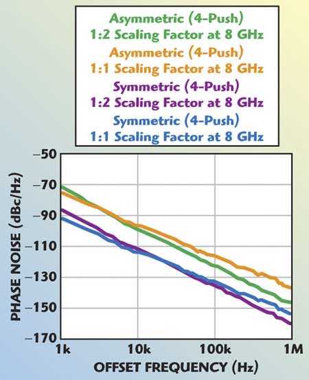
Fig. 9 Measured phase noise of the coupled 4-push VCO.
The novel approach allows for a substantial reduction in phase noise by dynamically minimizing the phase error and noise impedance transfer function of the planar-coupled oscillators network over the operating frequency band.7
The typical measured phase noise is better than –90 dBc/Hz at a 10 kHz offset from the carrier.3 Competing other alternative semiconductor technologies may not deliver the same level performance in terms of cost, size, power, linearity, tunability, adaptability, reconfigurability and integrability for this class of VCOs using scaled devices.
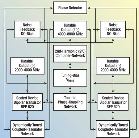
Fig. 10 Block diagram of a coupled mode 2-push, 2 to 8 GHz VCO (patented).
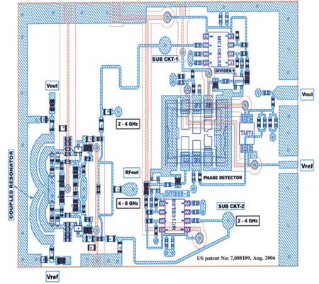
Fig. 11 Layout of a coupled mode 2-push, 2 to 8 GHz VCO (patented).
ConclusionThe multi-octave band design approach based on device scaling and optimum symmetry of the signal waveforms demonstrated in this work enables wide tuning, extended frequency of operation and lower phase noise performance, which are attractive for present industry applications.
This article describes the impact of device scaling on phase noise in coupled oscillators, which have recently emerged as strong contenders for radio frequency (RF) and mixed-signal applications. Ulrich
L. Rohde studied electrical engineering and radio communications
at the Universities of Munich and Darmstadt, Germany. He holds his
PhD degree in electrical engineering (1978) and his Sc.D. (hon. 1979)
in radio communications, his Dr.-Ing. (2004) and several honorary
degrees. He is president of Communications Consulting Corp.; chairman
of Synergy Microwave Corp., Paterson, NJ; and a partner of Rohde & Schwarz,
Munich, Germany. He was previously president of Compact Software
Inc., Paterson, NJ, and business area director for radio systems
of RCA, Government Division, Camden, NJ. He is a professor of microwave
circuit design and has held visiting professorships at several universities
in the United States and Europe.
Ulrich
L. Rohde studied electrical engineering and radio communications
at the Universities of Munich and Darmstadt, Germany. He holds his
PhD degree in electrical engineering (1978) and his Sc.D. (hon. 1979)
in radio communications, his Dr.-Ing. (2004) and several honorary
degrees. He is president of Communications Consulting Corp.; chairman
of Synergy Microwave Corp., Paterson, NJ; and a partner of Rohde & Schwarz,
Munich, Germany. He was previously president of Compact Software
Inc., Paterson, NJ, and business area director for radio systems
of RCA, Government Division, Camden, NJ. He is a professor of microwave
circuit design and has held visiting professorships at several universities
in the United States and Europe.
 Ajay
K. Poddar graduated from NIT Calicut (1991), IIT Dehli (1996)
and obtained his PhD degree (Dr.-Ing) from the Technical University
Berlin, Germany, in 2005. He is a chief scientist, responsible for
the design and development of new, state-of-the-art technology (oscillator,
mixer, amplifier, filters and MEMS-based RF components) at Synergy
Microwave Corp., Paterson, NJ. He previously worked as a senior scientist
in DRDO (Defense Research and Development Organization), India, from
1991 to 2001.
Ajay
K. Poddar graduated from NIT Calicut (1991), IIT Dehli (1996)
and obtained his PhD degree (Dr.-Ing) from the Technical University
Berlin, Germany, in 2005. He is a chief scientist, responsible for
the design and development of new, state-of-the-art technology (oscillator,
mixer, amplifier, filters and MEMS-based RF components) at Synergy
Microwave Corp., Paterson, NJ. He previously worked as a senior scientist
in DRDO (Defense Research and Development Organization), India, from
1991 to 2001.