Inductors are a necessary building block in many circuits, including oscillators. Because passive spiral inductors can occupy a large amount of real estate in integrated-circuit (IC) designs, the search has been on for smaller, tunable active inductors (TAIs) suitable for monolithic fabrication. While smaller than passive inductors, TAIs have often meant a sacrifice in linearity and phase noise. To overcome this hurdle for creating smaller, lower-noise tunable voltage-controlled oscillators (VCOs), Synergy Microwave has developed TAI-based VCO circuits that employ dynamic phase injection so that the active inductance value changes monotonically with control voltage without degrading linearity or phase noise. Experimental oscillators suitable for high levels of integration have been fabricated using this approach, with measured phase noise of better than -110 dBc/Hz offset 1 MHz from a 12-GHz carrier. The 12-GHz VCO features a 200-MHz tuning range while requiring only 12 mA and +3-VDC bias.
Radio-frequency integrated circuits (RFICs) and monolithic- microwave integrated circuits (MMICs) are often implemented in planar configurations. As is often the case, passive spiral inductors tend to dominate the real estate of these designs because of their large size, limiting the cost-effectiveness of certain designs, such as amplifiers and oscillators, especially when fabricated on expensive substrate materials such as gallium arsenide (GaAs).
Ideally, those large spiral inductors could be replaced by an active inductor based on transistors and occupying only a fraction of the amount of substrate area as the passive spiral inductors. The active inductors should also provide equal if not better performance at microwave frequencies as the passive inductors. But first, one of the traditional limitations of active inductors that must be overcome is the added noise from the active devices, which can impact the performance of various components, including the phase noise of tunable oscillators.
A great deal of effort has already been devoted to creating high-qualityfactor (high-Q) resonator networks for integrated tunable oscillators using active inductor technology. 1-8 An activeinductor- based resonator has the same state equation as a passive inductorcapacitor (LC) resonator, along with gain and some scaling terms to compensate for the loss resistance, R, associated with a passive LC resonator. Because active inductors are based on active semiconductor devices, they require a certain amount of power to realize an inductor with negative resistance, and so will always be more dissipative than their passive inductor equivalents.
It is also reasonable to expect that an active inductor will also suffer higher root-mean-square (RMS) noise than a passive inductor. The noise in an ideal passive resonator, represented by an inductor, capacitor, and associated resistance, R + , or LCR + , arises from power dissipation through the loss resistance, R loss = R + . The mean square voltage of the thermal noise on a capacitor, kT/C, appears across the passive resonator (LCR + ) regardless of the magnitude of resistance R.
The selectivity of a passive resonator (? 0 /Q) is established by the dissipation, according to the relationship 1/Q = (? 0 L/ R + ). Since noise sets the lower limit for detecting a signal in a resonator network, the upper limit may be arbitrarily large if the resonator network is assumed to be free from inductor saturation or other possible linearity issues.
Tunable active inductors (TAIs), if properly implemented, offer great promise for high-performance, miniaturized tunable oscillators in RFIC and MMIC technologies. Unfortunately, they have been plagued by a number of disadvantages compared to passive inductors with comparable values when implemented in those technologies, including higher noise, lower dynamic range, higher power consumption, lower self-resonant frequency (SRF), and limited tuning bandwidth. Clearing these hurdles is critical to a more effective use of TAIs in ICs, for example in oscillators where improved Q can provide enhanced performance and for tunable filters where dynamic range is important. By using active circuitry, it may be not only to generate an on-chip inductance value of a much larger spiral inductor, but to also provide the characteristics needed to achieve low phase noise in highfrequency VCOs.
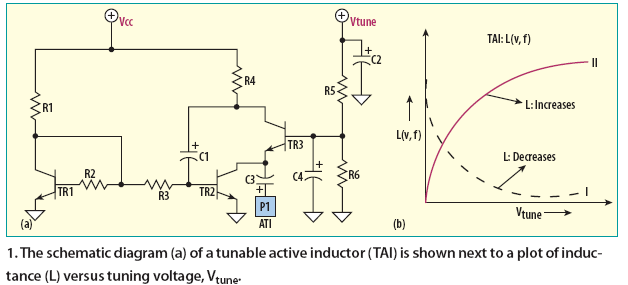
A schematic diagram for an active inductor based on silicon germanium (SiGe) heterojunction-bipolar-transistor (HBT) technology is shown in Fig. 1(a), along with its tuning characteristic in Fig. 1(b). The slope of inductance with control voltage and frequency can be negative, where inductance decreases with control voltage, or positive, where inductance increases with control voltage, depending upon the TAI topology. Both tuning curves indicate strong nonlinearities under large-signal drive conditions, which have long plagued the widespread use of TAIs in highfrequency ICs.
A TAI-based 12-GHz VCO based on SiGe HBT technology was developed with an active capacitor in an attempt to improve noise performance and dynamic range (not shown). For a high dynamic range, the inductor must handle relatively high power levels with low distortion. Most tunable inductors in the technical literature rely on adjusting the bias point of an active device, using the device’s transconductance (gm) as the tuned value. Unfortunately, transconductance is not linear with bias under large-signal conditions, making it almost impossible to achieve good linearity with this approach.
The history of the TAI is relatively long and often based on the use of a gyrator. Early work can be traced to Dutch theorist B.D.H, Tellegen of Philips. A basic circuit using a reactance tube was designed in 1930 for electronic tuning and FM generation. Earlier researchers noted that a TAI was subject to largesignal limitations and other problems.3 An active inductor based on a gyrator can be realized by connecting inverting and non-inverting amplifier back-toback in parallel.
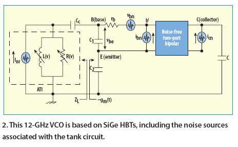
A schematic diagram for a TAI based on SiGe HBTs, including the noise sources associated with the TAI tank circuit, is shown in Fig. 2. Part of the negative resistance, [Rv(t)], generated by the TAI can be used to minimize an oscillator’s dynamic noise. It can lower the oscillator’s power consumption by means of a reduction in the RF output current duty cycle.
A typical TAI consists of a grounded active inductor, a cascade grounded inductor, and a resistive-feedback active inductor that can be implemented as part of an RFIC or MMIC. Such a circuit can be used in power dividers, quadrature couplers, and oscillators, provided it has adequate voltage-handling capability and is not current limited like a passive inductor. Unfortunately, this approach has limited dynamic range and tuning range resulting in only narrowband operation.
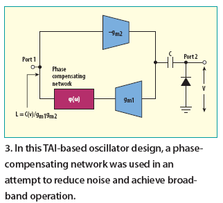
For oscillator and frequency synthesizer applications, it is critical that a TAI provide a wide tuning range. To achieve this, a modified TAI incorporates a dynamic phase compensating network to achieve broadband operation ( Fig. 3). In this modified design, the gyrator converts capacitance C(v) into inductance L(v) as a function of delay (f) and control voltage, V 1 , according to
L(v) ˜ C(v)/(g m1 g m2 ) (1)
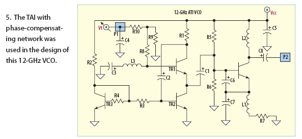
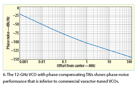
A schematic diagram for the TAI and phase-compensating network is shown along with a Smith chart tracing the complex impedance in Figs. 4(a) and (b). . The chart indicates inductive behavior from 600 MHz to 30 GHz, although the real part of the input impedances are positive everywhere, indicating lossy operation. Point 3 in the chart is sensitive (at 4.3 GHz) and should not be encircled, which can limit some applications. The TAI was used in the design of a 12-GHz VCO ( Fig. 5 ) and its phase noise was plotted ( Fig. 6 ). The phase noise, of -100 dBc/Hz offset 1 MHz from 12 GHz, is far from impressive and not as good as commercially available varactor-tuned VCOs. 9

Several approaches to overcome these problems have been considered, such as minimizing the noise introduced by the active devices in the TAI circuits.1-9 However, even these techniques result in power-hungry and band-limited characteristics because negative resistance generated in series with the inductance is not constant with operating frequency. The approach of using TAIs with dynamicphase- injection techniques, however, can improve oscillator phase noise without degrading the linearity.
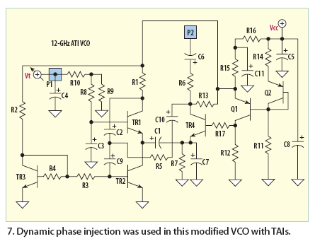
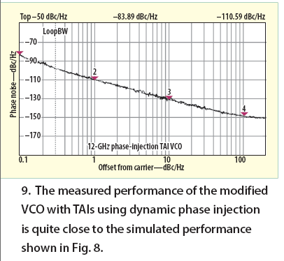
To demonstrate the effectiveness of using dynamic-phase-injection techniques with a TAI, a 12-GHz VCO employing TAIs with dynamic phase injection was fabricated on a dielectric circuit board from Rogers Corporation . The substrate material was 30 mils thick with a dielectric constant of 3.38 in the z-direction at 10 GHz. The schematic diagram for this improved TAI-based VCO is shown in Fig. 7 while a simulated phase-noise plot is shown in Fig. 8 . Compared to the performance of the unmodified (but phase compensated) TAI-based VCO of Fig. 5 , this new design shows 10 to 15 dB improvement in phase noise. The use of dynamic phase injection minimizes oscillator noise while simultaneously decreasing the current consumption, so that users no longer have to balance a tradeoff between phase noise and power consumption. Measurements on the oscillator circuit ( Fig. 9 ) show that the actual phase noise is within 3 dB of the simulated performance, while achieving a tuning range of 200 MHz with only 12 mA and +3 VDC bias.

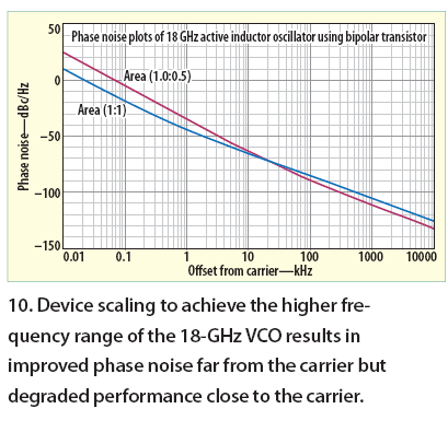
To further explore the use of TAIs with dynamic phase injection in highfrequency oscillators, scaling was used to achieve a higher-frequency oscillator by increasing the cutoff frequencies of the transistors. Based on 1.0:0.5 device-scaled SiGe HBTs, a TAI-based oscillator designed for use at 18 GHz shows a 20-percent tuning range. As Fig. 10 indicates, device scaling increases the noise contribution from 1/f noise (close to the carrier) while decreasing contributions from base current shot noise and base resistance thermal noise (far from the carrier). The result in the 18-GHz oscillator design is a typical 8-dB degradation in close-in phase noise (1 kHz offset from the carrier) with a 5 dB improvement in phase noise further from the carrier (10 MHz offset from the carrier), using SiGe transistors scaled to one-half their normal size.
Still, the results shown for the 12-GHz VCO based on TAIs with dynamic phase injection are promising. Those results indicate that TAIs can be applied to the fabrication of miniature high-performance monolithic oscillators to achieve excellent phase-noise levels without sacrificing linearity or power consumption.