Various reference oscillator schemes are possible as shown in Figure 1.5 A 10 MHz temperature-compensated crystal oscillator (TCXO) provides small size and low cost benefits for low-to-moderate performance applications, but higher multiplication factors can degrade the noise floor significantly. Improved stability and phase noise performance can be achieved by using a 100 MHz oven-compensated crystal oscillator (OCXO), but at the cost of size and power consumption. It is worth noting that higher frequency OCXO (for example, 100 MHz instead of 10 MHz) can potentially result in a improved synthesizer jitter and phase noise performance. Frequency multipliers are used to extend synthesizer operating frequency bands, but at the cost of phase noise and spurs, which are degraded at 20logN, where N is the multiplication factor. Therefore, a design er's main concern is to minimize the degradation of phase noise using self-injection and noise filtering techniques, and the most effort is toward the realization of developing fundamental low phase noise high reference signal sources.7 Figure 2 shows the measured phase noise plots for a 128 MHz VCXO circuits (VCXO #1, Vtune=2 V; VCXO #2, Vtune=5 V; VCXO #3, Vtune=2 V; VCXO #4, Vtune=5 V) to provide a brief insight about the phase noise characteristics.
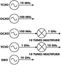
Figure 1 Typical reference frequency generation topology.
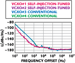
Figure 2 Measured phase noise plots of 128 MHz VCXO circuits.
As shown in Figure 2, self-injection feature adjusts the phase of the resonator tank for providing optimum group delay, thereby improving the phase noise below 1 kHz offset from the carrier. Further improvement in phase noise performance at far offset (< 1 kHz) can be achieved by an adaptive self-tuning filter network that introduces the required delay to generate a feedback signal for far out phase noise reduction.3-7
Multiplied Frquency Crystal Oscillator Circuit
As briefly discussed, designers have often relied on multiplying a low-noise crystal oscillator to achieve higher frequency 1 GHz and higher output signals. The harmonic frequency crystal oscillator approach can provide excellent phase noise, but tends to consume a great deal of power, generate high levels of noise, and are large in size. Commercially available crystal oscillators at 100 MHz and below are available with phase noise of -160 to -176 dBc/Hz offset 20 to 100 kHz from a 100 MHz output.
When multiplied 10 times to obtain a 1 GHz frequency source, the phase noise of crystaloscillators translates to -140 to -156 dBc/Hz offset 20 to 100 kHz from 1 GHz but can degrade the noise floor by as much of 20 dB. The availability of low cost, low noise voltage-controlled saw oscillators (VCSO) clears the way for small, low noise synthesizers. Part of using these sources involves modeling the surface acoustic wave resonators under large signal drive conditions for better insights about noise dynamics at close-in phase noise, then developing manufacturable methods for producing high-purity and temperature stable oscillators in chip form.
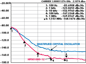
Figure 3 Performance comparison between a 1 GHz VCSO and a multiplied crystal oscillator.
Figure 3 compares a fundamental 1 GHz VCSO (HFSO1000-12)phase noise at 1 GHz to that of a commercially available multiplied crystal oscillator circuit. It can be seen that a fundamental 1 GHz VCSO supersedes the phase noise performance as much as 20 dB at 100 kHz offset from the carrier as compared to commercially available multiplied 1 GHz VCXO. The primary drawback of VCSOs is their inability to be tuned by means of tuning varactor diode; therefore, they are unable to compensate the frequency drifts due to aging and changes in operating temperature for reference source applications. Accordingly, there is a need for frequency agile SAW resonators for VCSO applications.
In this article, new techniques using degenerated adaptive mode-coupling and regenerative noise filtering are being incorporated to achieve excellent spectral performance at fundamental frequencies of 3 GHz and above. The novel approach includes a methodology to enhance the mode-injection locking range using delay feedback techniques and to reduce or eliminate the amount of filtering needed to suppress sub-harmonics and higher-order harmonic products. The approach also reduces the susceptibility to microphonics while retaining low phase noise and a moderate tuning range to compensate for short-term and long-term effects of thermal drift and aging.2 The reported reference sources are ideal for use as clock translators for high speed analog-to-digital converters (ADC) and direct-digital-synthesizer (DDS) clocks, offer superior figure-of-merit (FOM) in terms of performance, price, and product delivery to satisfy both the technical and current business needs of designers and buyers.
Adaptive Harmonically Tuned Reference Signal Source Topologies
High Q factor resonator (RF-MEMS, Crystal, SAW, Ceramic) based oscillators are widely used in wireless applications because the technology features very low phase noise at fixed frequencies through about 1 GHz. However, a reference signal source operating above 1 GHz is generally realized using a multiplier approach, which is power hungry, large in size and has degraded phase noise performance. Figure 4 shows the typical block diagram of the ultra low phase voltage-controlled oscillator using an adaptive mode-coupled harmonically tuned mechanism enabling more than 500 kHz tuning for compensating the thermal drift without using a heating device and fabricated in tiny SMD packages (0.5" × 0.5").
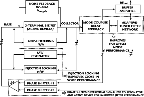
Figure 4 Block diagram of an adaptive mode-coupled, harmonically toned VCSO.
The typical measured phase noise of a harmonically tuned (5th harmonic) 1 GHz SAW resonator at 10 kHz offset from the 5 GHz carrier is -138 dBc/ Hz, with RMS jitter less than 10 femto sec. The reported harmonically tuned 5 GHz VCSO offers about 10 to 15 dB superior phase noise performance as compared to commercially available SAW and crystal multiplied sources for a given size, cost and power consumption.
Tunable SAW Resonator For VCSO Circuits
The resonant frequency of the SAW device is set by the distance between the electrode "fingers" (see Figure 5). Quartz, LiTaO3 and LiNbO3 are common substrates for such devices. Initial accuracy is dependent on the accuracy of the printing of the "fingers." Initial accuracy can be in the ±50 to 200 ppm range. The approximate temperature constant of quartz is 0.03 ppm/0C² and -20ppm/0C² for LiTaO3.
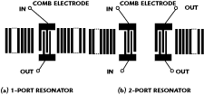
Figure 5 Typical representation of SAW resonator (a) one-port saw and (b) two-port saw.
Generally, it is highly desirable for reference frequency sources to exhibit ultra low phase noise characteristics. This is usually accomplished by using high Q quartz crystals and SAW resonator devices. Unfortunately, SAW resonator based oscillators have several disadvantages, including a limited operating temperature range and limited tuning range (which limits the amount of correction that can be made to compensate for the tolerances of other components in the oscillator circuitry). Coupling a varactor diode or other capacitive element to a high Q-factor frequency controlling element, such as SAW device, does not result in a tunable, low phase noise VCSO circuit. To overcome this limitation, VCSO have been implemented that couple together two or more SAW devices to achieve a wider tuning range and low phase noise. The simplified approach is to reduce the quality factor of the SAW by introducing series or parallel loss resistors. However, the use of multiple SAW elements increases the complexity and the cost of the VCSO circuits.
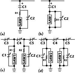
Figure 6 Arrangements of tunable SAW resonator networks.
Figure 6 shows the arrangement of tunable SAW resonator network based on the design trade-offs between the phase noise and the tuning characteristics of the VCSOs. Although the frequency of VCSO can be changed over a fairly wide range by means of varying the capacitances (C1 to C5), the parameters of the oscillator circuit are changing drastically. Figure 6 shows the arrangements of tunable SAW resonator networks: (a) series resistance in conjunction with SAW resonator, (b) parallel series resistance in conjunction with SAW resonator, (c) series resistance in conjunction with capacitively coupled SAW resonator, and (d) parallel resistance in conjunction with capacitively coupled SAW resonator.
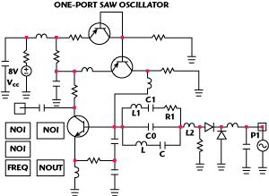
Figure 7 Schematic of a typical SAW resonator oscillator.
This creates serious problems in terms of phase noise and tuning linearity. For low phase noise, it is necessary to keep the reactance slope as steep as possible by maximizing the phase derivative and group delay (?f/??) of the coupled SAW resonator network. For tuning linearity, it is necessary to keep the reactance slope as straight as possible over the desired operating frequency range. If the reactance curve is too shallow, the oscillator circuit becomes susceptible to noise and stability perturbation. Furthermore, the straighter the reactance curve is, the greater is the tuning linearity in the desired frequency range. To overcome these problems, a novel technique is to incorporate additional inductor (L) parallel to the SAW resonator that resonates with the C0 (the internal and package capacitance of SAW resonator) as shown in Figure 7. Additionally, the value of inductor L2 and C is adjusted in order to shift the resonance to that of intrinsic SAW resonator (without insertion of L and C) frequency (i.e. 1 GHz). This enables the reactance curve linear and steep over the operating frequency range from 999.3 to 999.8 MHz.
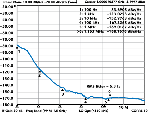
Figure 8 Phase noise of a cascaded mode-coupled, harmonically tuned SAW resonator oscillator (999 to 1001 MHz).
An objective of this design is to improve the tuning characteristics (on the order of ±400 ppm) of the SAW resonator without compromising phase noise performance by cascading the mode-coupled harmonically tuned network to compensate the frequency drift caused due to change in operating temperature (-40° to +85°C). The drive to maximize the phase noise performance using a mode-coupled harmonically tuned network in the compact space is particularly demanding on the RF/microwave communication systems. The cascaded mode-coupled harmonically tuned VCSO circuit minimizes the phase noise with more than 2 MHz tuning, resulting in a cost-effective solution. The typical measured phase noise is -152 dBc/Hz at 10 kHz offset from the carrier with jitter less than 6 fs, this is the reasonably low phase noise solution for this class of inexpensive VCSO solutions (see Figure 8).
Ultra Low Phase Noise Signal Source Design Methodology
The oscillator design methodology is being traded simultaneously by an increase in operating frequency, bandwidth and a decrease in physical size. The result is that the physical design layout challenges faced by circuit designers are rapidly increasing, while choices for how these challenges should be best-addressed are kept aside. In addition, oscillator design technology did not earn its reputation as black magic for no reason.
Unlike other microwave circuits, oscillators do not behave in a totally predictable way, so "tweaking" has been an accepted mainstay of the signal sources design flow. Fortunately, high frequency commercial CAD design tools (Agilent, Ansoft, AWR, MS Office, MathCAD, etc.) have dramatically improved so that tweaking of prototype circuits is much less common, and today's designers have powerful CAD tools that can make meaningful sense of the black magic.
For high Q factor resonator based oscillator applications, noise dynamics place stringent conditions on these reference frequency sources owing to inherent high noise figure and low dynamic range caused by the uncontrolled nonlinearity at large-signal drive-level conditions. In addition, these problems become critical at high frequency when active devices (bipolars/FETs) are technologically scaled to obtain higher cut-off frequency. Historically, nonlinear devices have been represented in simulation by compact empirical or analytical SPICE models that operate in the time domain. The linear portion of the network is being analyzed in the frequency domain and the nonlinear components in the time domain, resolving the two through an iterative technique called harmonic balance. However, most device parameters are extracted from linear 50 O S-parameters and DC I/V (static and pulsed) data. Their ability to predict behavior under extreme nonlinear conditions or non-50 O terminations, especially for autonomous circuits, is questionable.
The definition of S-parameters in large-signal environment is ambiguous compared to small-signal S-parameters. When driving an active device with an increasingly higher level, the output current consists of DC and RF currents, the fundamental frequency and its harmonics. When increasing the drive level, the harmonic content rapidly increases. S12, mostly defined by the feedback capacitance, now reflects harmonics back to the input. If these measurements are done in a 50 O system, which has no reactive components, then we have an ideal system for termination. In practical applications, however, the output is a tuned circuit or matching network, which is frequency selective. To measure large-signal S-parameters, the device was mounted to a test fixture that was calibrated to provide 50 O to the transistor leads. The test set-up consisted of a DC power supply and a network analyzer for combined S-parameter measurements. The R&S ZVR network analyzer was chosen because its output power can be swept from +10 to -60 dBm.
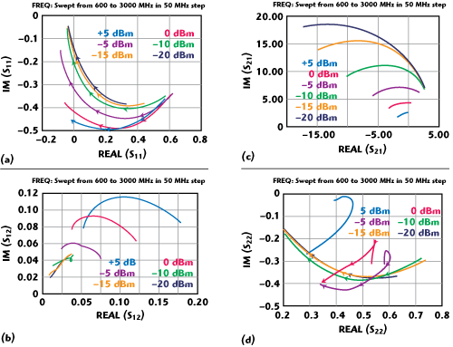
Figure 9 Measured large-signal S11 (a) S12 (b) S21 (c) and S22 (d) of the bipolar transistor.
Figure 9 shows the plot of the measured S-parameters under large-signal drive condition for the characterization of oscillation condition and noise dynamics of the oscillator circuits. However this exercise is time-consuming and, therefore, not cost-effective. Fortunately, commercially availableAgilent Technologies X-parameters could measure large-signal S-parameters that describe nonlinear behavior of the active device and can correlate the spectra found at a device's terminals for a given set of stimuli and termination impedances. Therefore, tweaking of prototype circuits is much less common, and today's designers have powerful CAD tools that can make meaningful sense of the nonlinear characteristics of the active circuitry.
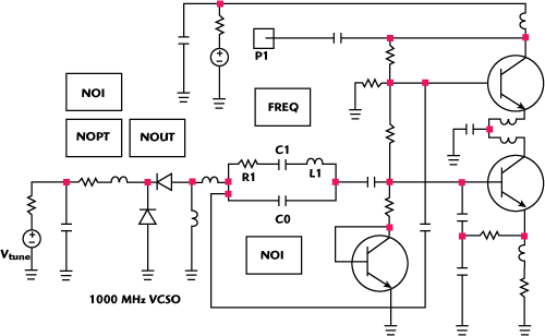
Figure 10 Schematic of typical tunable mode-coupled 1 GHz SAW resonator oscillator.
Figure 10 shows the schematic of tunable 1 GHz SAW oscillator circuit, designed using large-signal S-parameters measured at different drive-levels. The CAD simulated phase noise confirms the improvement in performance at 1 kHz and higher offset frequency from the carrier and validated with experimental results shown in Figure 11.
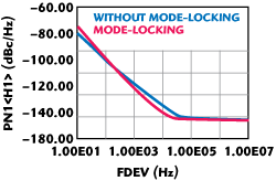
Figure 11 Phase noise plot of mode-coupled tunable 1 GHz SAW resonator oscillator.
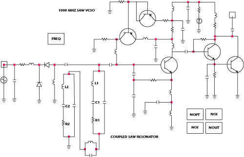
Figure 12 Schematic of typical tunable hybrid mode 1 GHz SAW resonator oscillator.
Figure 12 shows the schematic of hybrid mode tunable 1 GHz SAW oscillator. For comparative analysis and brief insights about the various topologies, Figure 13 shows the measured phase noise plots of tunable SAW oscillators. It can be seen from the figure, injection-mode coupled VCSOs offer promising phase noise with 1 MHz tuning to compensate the ageing and frequency drift. The drawback of this approach is vibration sensitive VCSO circuit. Care must be taken for the application where g-sensitive criteria is an important yard stick. By properly packaging and securing the SAW resonator in the cavity using double layer PCB for compensating the temperatrre charateristics, g-insensitive solutions can be produced.
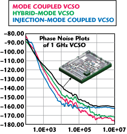
Figure 13 Measured phase noise plots of tunable SAW oscillators.
Conclusion
The new ultra low phase noise VCSOs offer significant promise in terms of performance, price and product delivery to satisfy both the technical and business needs for low cost, low phase noise high frequency reference sources for synthesizer applications.
Historically, synthesizer developers have relied on a crystal based multiplied 1 GHz reference oscillator featuring excellent phase noise performance at frequencies of 3 GHz and above. A frequency multiplier crystal oscillator can offer low phase noise performance at frequencies of 1 GHz and above, but at the cost of larger size, higher noise floor and higher power-consumptions.1-7 The most dramatic change will occur when optimum loop bandwidth extends to a few megahertz, where reported adaptive mode-coupled harmonically tuned voltage controlled SAW oscillator (VCSO) noise performance supersede the performance of the conventional VCSOs and dielectric resonator oscillators (DRO), including the multiplied crystal oscillators at 3 GHz and above. Ulrich L. Rohde, Ajay Kumar Poddar | September 2011 | Microwave Journal Magazine