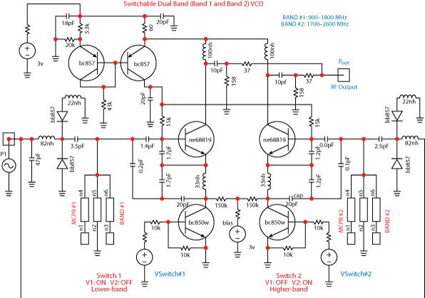
Fig. 1 Typical schematic of a dual-band
switched oscillator.
Mobile phones and radios, operating in several modes, are typically switching between receiving and transmitting frequencies, and therefore require low phase noise signal sources (oscillators/VCOs) in each of the respective switched bands.
It is known that the oscillators exhibit trade-offs between power consumption and phase noise. To reduce the phase noise, power consumption and real estate area are increased.
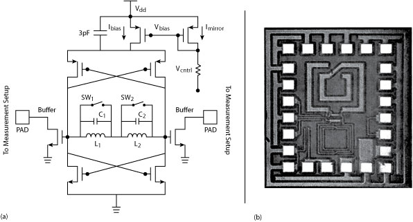
Fig. 2 A dual-mode oscillator’s
(a) schematic and (b) chip photograph.
To miniaturize the system and reduce the power consumption, multi-band, multi-mode system designers are forced to explore a frequency plan that employs one or more oscillators, phase-locked loop (PLL) frequency dividers, buffer amplifiers, filters, switching architectures and multipliers.
The miniaturization and the merging of multi-band systems impose stringent requirements on size, power, performance and configurability of the fully integrated transceiver systems.
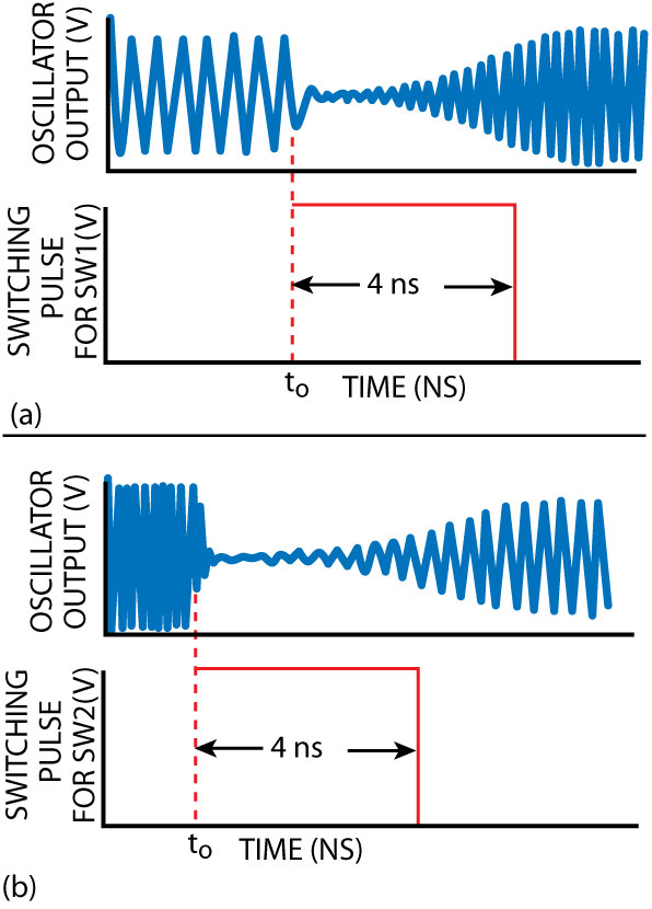
Fig. 3 A dual-mode oscillator’s
mode 1 and mode 2 outputs.
The technology of the wireless devices also must allow for a smooth migration to future generations of communication standards with higher data rates.
Hence, the compact and power-efficient implementation of such multi-standard terminals calls for the need of an intelligent RF front-end that can achieve maximum hardware sharing for various standards.
Such a compact RF front-end would require reconfigurable multi-band VCO blocks rather than frequency multiplier or divider or switched resonator architectures.
Various techniques, such as switching between VCOs for separate bands, using inter-modal multiple frequencies and switched resonators for band selection have been proposed.1–25
However, these methods result in circuits of large size, which are current-hungry, narrowband and with poor phase noise performance. Figure 1 shows the typical schematic of a dual-band (Band 1: 900 to 1800 MHz; Band 2: 1700 to 2600 MHz) switched voltage-controlled oscillator, where the oscillators are alternatively switched with switches 1 and 2 to generate Bands 1 and 2.
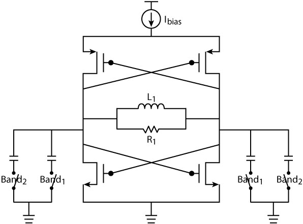
Fig. 4 Typical switched-resonator
oscillator.
Switched resonators (inductors or capacitor banks) suffer from the resistive and capacitive parasitics associated with the switches.
A recent paper2 shows a novel method of mode switching (see Figure 2) in which both switches SW1 and SW2 are open when any of the desired oscillation modes (mode 1: f1 = 2.398 GHz or mode 2: f2 = 4.733 GHz) are established.
This oscillator uses a cross-coupled CMOS device with L1 = 2.34 nH, L2 = 0.86 nH, C1 = 1.6 pF and C2 = 0.96 pF. Figure 3 demonstrates the concept of mode switching, assuming that both switches SW1 and SW2 are normally open and the circuit is oscillating at f1.
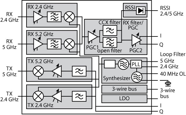
Fig. 5 Block diagram of a dual-band
transceiver.
In order to change the oscillation frequency to f2, SW1 is closed for only a short duration, thereby reducing the region of attraction for f1 and increasing it for f2, causing decay of the oscillations at f1 and growth of the oscillations at f2. Once the oscillations at f2 are stabilized, SW1 can be opened again. The system keeps oscillating at f2 thereafter, since it is one of its steady-state stable modes of oscillation.
As shown, SW1 is closed at t0 for 4 ns, enough for the oscillation at f2 to stabilize. In order to switch from f2 to f1, SW2 is closed for a small duration.
It is understood that when the desired oscillation mode (mode 1 or
mode 2) is established, both switches are open. Therefore, the loss
and nonlinearity of the switches do not degrade the steady-state and
phase noise performance of the oscillator.
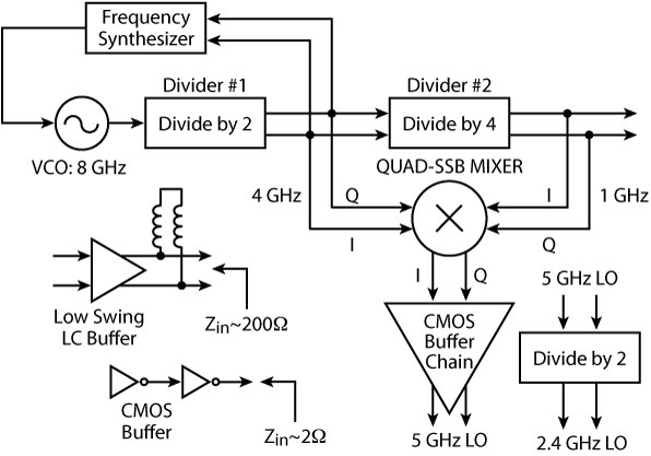
Fig. 6 Frequency plan for a 2.4/5 GHz WLAN transceiver.
This is fundamentally different from the traditional band-select oscillators, where the dual-band resonances are obtained by alternatively switching oscillators or switching inductors/capacitors (see Figure 4).10,20
The main drawback of such architecture is that the band-selecting switch is placed in the signal path and thus deteriorates the performance of the oscillator because of its loss and nonlinearity.
In the case of the switched mode oscillator, the switching mechanism is limited to a short duration (between the stable modes of oscillations), just to get the desired band, as opposed to switching between two capacitors or inductors.
However, the present solutions to the dual-band systems are not concurrent in a real sense, because the oscillators are alternatively switched between different resonators for generating the required different frequencies and the design technique does not allow the signals to be generated at the same time.
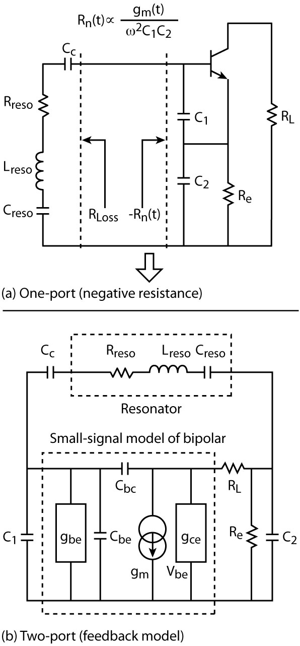
Fig. 7 One-port (a) and two-port (b)
approaches of a CE oscillator.
Therefore, they suffer from power consumption, larger area and design cycle time.
In this work, a novel technique is proposed, based on a dynamically controlled multi-mode oscillation technique using asymmetrical planar-coupled resonator networks to extend the tuning range of the oscillators.17,24
The proposed topology discussed in this article uses a new class of oscillator that generates multiple synchronous frequencies by using higher order (> 2), multi-coupled planar resonators (MCPR), which offers concurrent solutions by synchronously generating multiple frequencies for different bands without using a multiplier or switching resonators/oscillators network, therefore resulting in a reduction in power consumption, area and design cycle time.23–25
Theory
The next generation of wireless communication systems is supposed to be frequency agile and must be able to seamlessly span multiple frequency bands dynamically to cover different global standards.
Rapid evolution in the field of wireless communication and the convergence of multiple communication protocols has led to the integration of multiple complex functionalities in wireless portable devices.
Convergence of various standards, such as WLAN, into a motherboard of a computer or into a cell phone (3G and 4G) has led to added functionality in each system. The most commonly used frequency bands are the 2.4 to 2.5 GHz ISM band and several frequency bands from 5.15 and 5.85 GHz, with several communication standards defined in the IEEE 802.11 standards.
In order to give the user more freedom, phones that are able to cover more than one of these bands require reconfigurable concurrent signal sources for multi-band, multi-mode wireless communication systems.
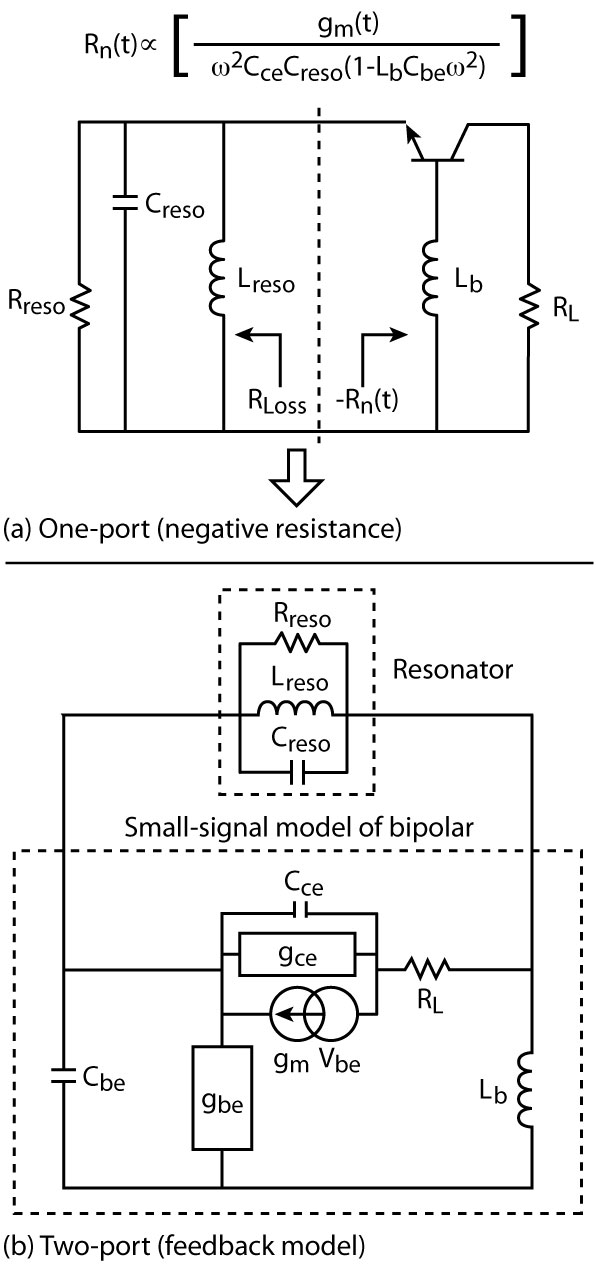
Fig. 8 One-port (a) and two-port (b)
approaches of a CB oscillator.
Figure 5 shows the typical schematic block diagram of a dual-band (2.4/5.0 GHz) transceiver system, where a single signal source (oscillator) with two or more frequency bands is the first step towards a fully integrated multi-band design.1 Figure 6 illustrates the divider and the switching-based architecture of the frequency plan for a 2.4/5.0 GHz WLAN transceiver system.8 As shown, the approach uses a single VCO at 8 GHz with a divider 1 (+ by 2) in a frequency synthesizer to generate a 4 GHz signal, which is followed by a divider 2 (+ by 4).
The output of divider 1 (4 GHz) and divider 2 (1 GHz) signals are mixed in a QUAD SSB mixer to generate the 5 GHz signal, which is further divided to obtain the required 2.4 GHz signal. The implementation utilizes multiple buffers, filters and divider networks.
Frequency multipliers can be an alternate option, but they are seldom used for the final stage of frequency conversion because of the difficulty in obtaining differential outputs at higher frequencies, which are required by quadrature converters.9,10 The basic principle of a multi-mode radio is to process two or more signals of differing frequencies at the same time, but using only one processing Tx-Rx chain.6,7
The nth-order (n > 2) MCPR-based, multi-mode RCO demonstrated in this work can satisfy the present demand for low cost, dual-band, low noise, power efficient, wide tuning range and compact size, and is easily amenable for integration in chip form.
Single Frequency Tunable Wideband Oscillator
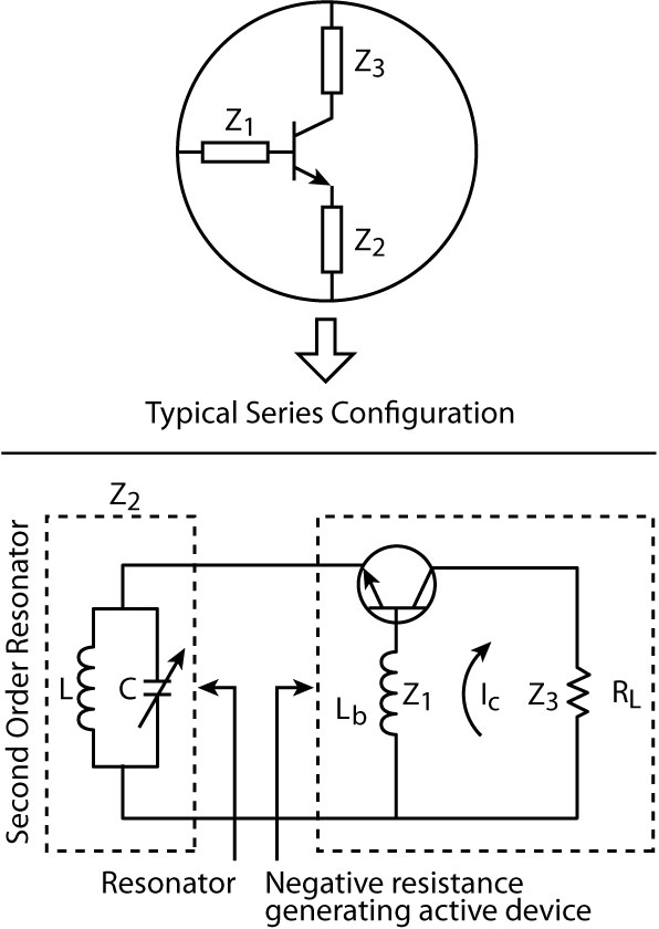
Fig. 9 General topology of
the series feedback LC-tuned oscillator.
Typical single frequency tunable oscillators use a grounded base or grounded emitter circuit for generating a negative resistance at one port, which is usually terminated with a parallel or series LC-resonant tuned circuit.
For wideband tunability, the required negative resistance over the band is generated by the feedback base-inductance (in the grounded base topology), but the polarity of the reactance may change over the frequency band and can lead to the disappearance of the negative resistance as the operating frequency exceeds its self-resonance frequency (SRF).
There are two primary constraints, which limit the oscillator circuit topologies: the first is the transistor and its package; the second is the large capacitance change required to tune the oscillator over an octave band.
The common emitter (CE) and common base (CB) are the common topology for a wideband VCO’s design. Figure 7 shows the CE topology, which uses a capacitive feedback network with C1 and C2 to create the negative resistance looking into the base of the transistor.3
Figure 8 shows the common base (CB) topology, which uses an inductor Lb in the base of the transistor to generate the negative resistance Rn(t) looking into the emitter of the transistor.4,17 As shown in the CE topology, small values of the feedback capacitances C1 and C2 generate a large negative resistance and allows for a wide tuning range at the cost of heavily loading of the resonator and wide conduction angle, hence poor phase noise performance.
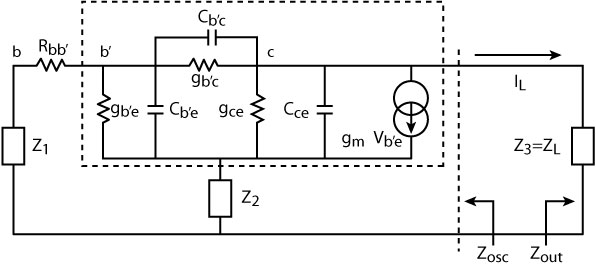
Fig. 10 Small-signal equivalent circuit
using a BJT.
For optimum phase noise performance, the active device is driven at a large-signal drive level that corresponds to a narrow conduction angle, and this restricts the lower limit of the feedback capacitors.
The drive level is directly proportional to the feedback capacitor C23; therefore, this topology is best suited for narrow tuning range (10 to 30 percent) VCOs because large values of feedback capacitors C1 and C2 will raise the loaded Q of the resonator at the expense of lesser tuning ranges and lower negative resistance.
The effective loading of the resonator for the common base (CB) oscillator configuration is due to the series combination of the load resistance and the transconductance of the transistor (the influences of gce, gbe and Cbe are neglected for simplification).
In this case, the loaded Q of the resonator is unaffected by the negative resistance generated by the feedback inductance Lb of the three-terminal device (bipolar/FET) and this configuration is therefore best suited for a wideband (octave-band) VCO application. Figures 9 and 10 show the general series feedback topology, and small-signal equivalent circuit for the purpose of the resonance frequency and noise analyses.
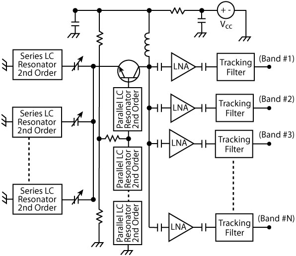
Fig. 11 Multi-band nth-order
oscillator (patent pending).
The steady-state oscillation condition for series feedback CB configuration is given by
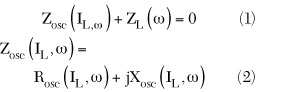
where
Rosc(IL,ω) = negative resistance components generated by the three-terminal active device (bipolar)
IL = load current amplitude
ω = resonance frequency
Zosc = current and frequency dependent output impedance
ZL = only function of frequency
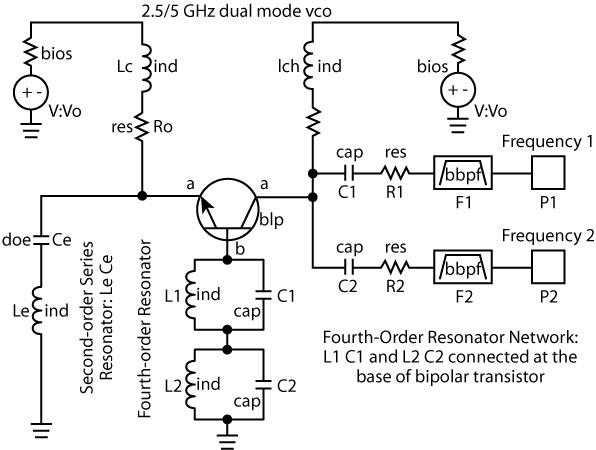
Fig. 12 Typical schematic of a dual-frequency
oscillator.
From Equations 1 and 2
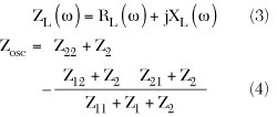
where Z11, Z12, Z21, Z22 are the [Z] parameters of the transistor. From Equation 4, Zosc, Rosc, Xosc and Rn can be given by
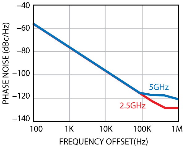
Fig. 13 Simulated phase noise
plot of the dual-frequency oscillator.
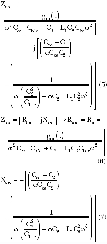
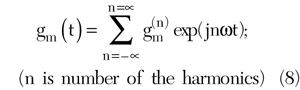
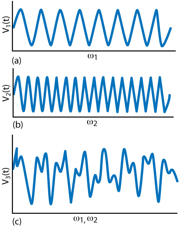
Fig. 14 Steady-state oscillations at w1, (a) and w2, (b), and simultaneous oscillations at w1 and w2 (c).
where
Rn = negative resistance of the series feedback oscillator
gm(t) = large-signal transconductance
The total noise voltage power within a 1 Hz bandwidth is3
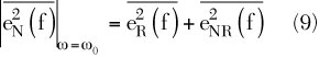
The first term of Equation 9 is related to the thermal noise, due to the loss resistance of the resonator tank, and the second term is related to the shot noise and flicker noise in the transistor.
From Equation 9, the phase noise can be described by3
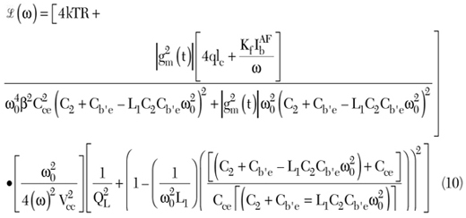
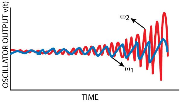
Fig. 15 Growth of oscillations at w1 and w2 when the time constant of resonator 1 (t1) is greater than the time constant of resonator 2 (t2).
where
 (ω)
= ratio of sideband power in a 1 Hz BW
(ω)
= ratio of sideband power in a 1 Hz BW
ω = offset frequency from the carrier
ω0 = resonance frequency
QL = loaded Q of the tuned circuit
Kf = flicker noise coefficient
AF = flicker noise exponent
kT = 4.1x10⁻²¹ at 300K
R = equivalent loss resistance of the resonator circuit
Ic = collector current
Ib = base current
Vcc = collector voltage
The performance of an oscillator can be evaluated by the figure-of-merit (FOM), and can be described by
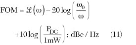
The first and third terms of Equation 11 represent the contributions of phase noise and power consumption (PDC) to FOM, respectively. From Equation 11, the phase noise for a given offset has greater impact on FOM than the power consumption does for a given oscillator frequency f0 (ω0 = 2πf0).
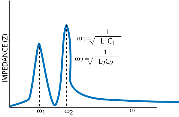
Fig. 16 Magnitude response of the dual-resonance network.
Multi-frequency (Multi-band and Multi-mode) Oscillator
Conventional oscillators are governed by second-order nonlinear differential equations and can only generate periodic waveforms, a single frequency and its harmonics. Oscillators with higher order nonlinear differential equations have multiple modes of oscillations and can generate multiple independent frequencies, individually or simultaneously.14–16
he paucity of literature on multi-ban, multi-mode oscillators, together with a lack of experimental verification of the underlying theories towards achieving the desired mode of oscillations in a controllable way, has been a strong motivator for research work.
The phase noise of higher order mode oscillators has not been investigated previously either.2 A single frequency tunable wideband oscillator utilizes a varactor-tuned, second-order resonator network (parallel LC or series LC network) to generate the desired frequency signal.
Fig. 17 Schematic of a dual-band concurrent oscillator.
The impedance response of the parallel LC and series LC resonator networks exhibit an anti-resonance (high parallel resistance: ideally infinite) and resonance (low series resistance: ideally zero resistance), respectively.
For simultaneous multi-frequency resonance, the order of the resonator network requires it to be increased, depending upon the number of frequency signals for the respective bands.
The main problems in this design are generating simultaneously a negative resistance over the multiple separate distinct bands. Figure 11 shows the typical simplified schematic of a multi-frequency (multi-band and multi-mode) oscillator of nth-order that can be explained with the help of the single band negative resistance approach.
From Equations 1 and 2, the steady-state oscillation condition for multi-band (nth-order) can be explained and described by
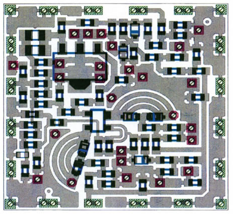
Fig. 18 Layout of the dual-band concurrent oscillator (patented).
where Rosc(IL, ω1, ω2, ω3…ωn) is the negative resistance components generated by the three-terminal active device (bipolar), IL is the load current amplitude, ω1, ω2, ω3…ωn are n distinct resonance frequencies, Zosc is the current and frequency dependent output impedance and ZL is only the function of frequency.
Dual-band, Dual-mode Oscillator
The idea of negative resistance in a single band oscillator was extended to a dual-band oscillator by Schaffner,15,19 where the oscillator has to simultaneously satisfy the resonance conditions for two distinct frequencies f1 and f2, respectively. Schaffner15 investigated mathematically the possibility of simultaneous oscillations at two independent and dependent frequencies based on a nonlinear negative resistance active device connected across a higher order (n = 4) parallel LC resonator network. Schaffner investigated both synchronous (f2/f1 = p/q = integer (⇒ rational number) and asynchronous (f2/f1 = p/q ≠ integer (irrational number) simultaneous oscillations in oscillators using differential equations.
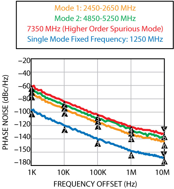
Fig. 19 Measured phase noise of the dual-band concurrent oscillator.
The method is a general method for determining sufficient conditions for the existence and stability of periodic solutions of a class of nonlinear vector differential equations. For transient analysis, the fourth-order system is broken into two second-order systems and the superposition theorem is applied to obtain the desired solution for dual-mode signal generations at frequencies f1 and f2. The independence of the frequencies is related to the irrational ratio of the frequencies (f2/f1 ≠ integer), whereas a rational ratio between the two frequencies (f1 and f2) implies that the signals are dependent on each other through their phase. Figure 12 shows the typical schematic of a dual frequency oscillator that uses a higher order of resonator network (fourth-order instead of second-order, LC resonant circuit, for a single frequency oscillator). From Equations 12 and 13, the oscillator circuit has to satisfy the necessary condition for guaranteed stable oscillations for two frequencies (f1 and f2). At a given frequency, the impedance with a negative real part is observed at the emitter terminal by adding an inductor of suitable value at the base terminal. The design philosophy for single frequency oscillation can be extended to apply to dual frequency oscillations. The fundamental criterion is to support simultaneously negative resistance at two distinct frequencies by synthesizing two inductors of different values. For stable oscillations, the resonator network at the base of the transistor terminal should be designed to provide different values of inductance (two degrees of freedom) at the desired center frequencies. Intuitively, a higher inductance value will be needed at f2 and a relatively lower inductance value is required at f1 (f2 > f1). Since a simple parallel LC network is insufficient to provide such a behavior, a fourth-order resonator is synthesized using L1–C1 and L2–C2. In general, a parallel-connected LC resonator will be inductive before the tank resonance (anti-resonance) and capacitive after the resonant frequency. At a given frequency the effective inductance (Leff) can be determined from a parallel-connected resonator by performing network analysis to calculate the Zin of a resonator. Figure 13 shows the simulated phase noise plot of the dual frequency (2.5/5.0 GHz) oscillator.
Validation
An oscillator with a high order (> 2) resonator has multiple stable modes of oscillations. By using a proper nonlinear active topology and resonator component values, the higher order oscillator (> 2) can generate more than one resonant frequency. For example, a fourth-order oscillator can generate either of the two distinct frequencies ω1 or ω2. Figures 14, 15 and 16 show the fourth-order oscillator that can generate either of the two distinct frequencies ω1 or ω2 or both ω1 and ω2. For validation purposes, the prototype is designed to generate two synchronous bands (fourth-order resonators) by incorporating two second-order parallel resonators in the base of the bipolar transistor.
Figures 17 and 18 show the schematic and layout of the reconfigurable dual frequency tunable concurrent oscillator18,25 that uses a fourth-order resonator network to satisfy the necessary conditions for guaranteed and stable oscillation conditions for two different frequencies (ω1, ω2) that can be tuned for two different frequency modes (bands) such as 2.45 to 2.65 GHz and 4.85 to 5.25 GHz. As a result, a simultaneous reduction in power consumption, area and design cycle time can be achieved using a concurrent solution.
The prototype is designed to generate two synchronous bands (fourth-order resonators) by incorporating two second-order parallel resonators in the base of the bipolar transistor. From Equations 12 and 13, the equivalent impedance at the emitter terminal must support a negative real part at two distinct frequencies (ω1, ω2). This can be achieved by synthesizing two inductors of different values at the base of the transistor corresponding to (ω1, ω2) for simultaneous sustained oscillation conditions. The resonator network at the base of the transistor (Q1) was designed in a MCPR medium to provide different values of inductance (two degrees of freedom) at the desired center frequencies.2–7 In general, a parallel LC resonator will be inductive before the tank resonance (anti-resonance) and capacitive after the resonant frequency. At a given frequency the effective inductance can be calculated from a parallel-connected resonator by performing network analysis to calculate the Zin of an equivalent resonator network. Since the active device (Q1) is sensitive to perturbations at all three nodes (base, emitter and collector) of the BJT, either of them can be tuned to obtain wideband tunability for different bands of oscillations for given values of RM1 and RM2 at P1 and P2. Intuitively, a higher inductance value is needed for Mode 1 (2.45 to 2.65 GHz), and a relatively lower value of inductance is required at Mode 2 (4.85 to 5.25 GHz). For wideband tunability, the effective values of inductance for different modes of oscillation are synthesized by incorporating a tuning capacitor across the resonators network at the base of the transistor Q in such a way that they provide the required negative resistance and reactance (inductive or capacitive) at the emitter terminal of the transistor Q over the required operating bands.25 Figure 19 shows the measured phase noise plot of the reconfigurable concurrent dual-band oscillators. The measured phase noise performance for Band 1 (2.45 to 2.65 GHz) and Band 2 (4.85 to 5.2 5 GHz) are typically better than –120 dBc/Hz at 1 MHz offset from the respective carrier frequencies. The circuit operates at 5 V, 20 mA and gives a typical output power of 3 dBm over the bands. The phase noise of the fourth-order oscillator, when generating only one of its resonant frequencies, is comparable to the phase noise of a second-order oscillator using the same active topology and resonator quality factor. Furthermore, the fourth-order oscillator has a better phase noise and/or a higher tuning range in VCO implementations, compared to the commonly used switched resonator oscillators.2 When the system begins to oscillate in dual-mode (Modes 1 and 2), a mode leakage occurs, and therefore how much mode leakage is allowed depends on the spectral selectivity of the succeeding filter and the system requirement.
Conclusion
The state-of-the-art, dual-band, multi-mode RCO reported in this article can be further extended to other higher stable mode such as triple-, quadruple- and nth-order modes. Hence, it can replace traditional multiple oscillators and the technology is compatible with existing IC process.
This article focuses on providing a cost-effective solution for multi-band, multi-mode wireless systems in which oscillators simultaneously satisfy the oscillation conditions of two or more signals, thereby obviating the need for several signal sources required for each phone. In multi-band, multi-mode radio architectures, a number of local oscillator (LO) frequencies are required in order to process the information in various frequency bands. It is known that local oscillators exhibit trade-offs between power consumption and phase noise performance. Since oscillators consume a substantial part of the chip area and battery power, this article describes the design approach of a reconfigurable concurrent oscillator (RCO) that simultaneously generates a dual frequency band, with the user having an option of choosing a distinct multiple frequency or a combination of them, which eliminates the need for lossy switches to switch the frequency band, thereby improving the system throughput. Ulrich
L. Rohde studied electrical engineering
and radio communications at the Universities of Munich and Darmstadt,
Germany. He holds his PhD degree in electrical engineering (1978)
and his Sc.D. (hon. 1979) in radio communications, his Dr.-Ing. (2004)
and several honorary degrees. He is president of Communications Consulting
Corp.; chairman of Synergy Microwave Corp., Paterson, NJ; and a partner
of
Ulrich
L. Rohde studied electrical engineering
and radio communications at the Universities of Munich and Darmstadt,
Germany. He holds his PhD degree in electrical engineering (1978)
and his Sc.D. (hon. 1979) in radio communications, his Dr.-Ing. (2004)
and several honorary degrees. He is president of Communications Consulting
Corp.; chairman of Synergy Microwave Corp., Paterson, NJ; and a partner
of  Ajay
K. Poddar graduated from NIT Calicut (1991), IIT Dehli (1996)
and obtained his PhD degree (Dr.-Ing) from the Technical University
Berlin, Germany, in 2005. He is a chief scientist, responsible for
the design and development of new, state-of-the-art technology (oscillator,
mixer, amplifier, filters and MEMS-based RF components) at Synergy
Microwave Corp., Paterson, NJ. He previously worked as a senior scientist
in DRDO (Defense Research and Development Organization), India, from
1991 to 2001.
Ajay
K. Poddar graduated from NIT Calicut (1991), IIT Dehli (1996)
and obtained his PhD degree (Dr.-Ing) from the Technical University
Berlin, Germany, in 2005. He is a chief scientist, responsible for
the design and development of new, state-of-the-art technology (oscillator,
mixer, amplifier, filters and MEMS-based RF components) at Synergy
Microwave Corp., Paterson, NJ. He previously worked as a senior scientist
in DRDO (Defense Research and Development Organization), India, from
1991 to 2001.