Frequency reference standards are essential to achieving frequency accuracy and phase stability in electronic systems. Such sources require the chief characteristics of low phase noise and good frequency stability.1-13 The best oscillator performance can be expensive, however. Fortunately, a patented approach has been developed to design and optimize the performance of voltage-controlled crystal oscillators (VCXOs), even those with relative low quality-factor (Q) resonators, to achieve excellent phase noise and frequency stability.
A typical oscillator consists of a tuned circuit and an active device such as a transistor. Ideally, the tuned circuit provides a high loaded Q, generally from less than 100 for simple circuits to more than 1 million for crystal-resonator-based circuits. Noise arises from the active device as well as from resonator losses. Noise from a bipolar transistor, for example, stems from base and collector contributions and from device parasitic elements, such as the base-spreading resistor. The filtering effect of the resonator tends to remove the device noise, with higher Qs delivering greater filtering effects. The Leeson equation relates these noise effects.1 The formula was modified by Rohde for use with VCOs.2
The equation is linear, with many unknowns. Among the more difficult oscillator performance parameters to predict are output power, noise figure, operating Q, and flicker corner frequency. The parameters can not be derived for linear conditions but require large-signal (nonlinear) analysis.3 But by combining Leeson's formula with the contributions of the tuning diode,2 Eq. 3 results, making it possible to calculate oscillator noise based on a linear approach:
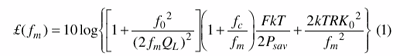
where:
£(fm) = the ratio of sideband power in a 1-Hz
bandwidth to the total power (in dB) at the frequency offset (fm);
f0 = the center frequency;
fc = the flicker frequency;
QL = the loaded quality factor (Q) of the tuned circuit;
F = the noise factor;
kT = 4.1 10–21 at 300°K (room temperature);
Psav = average power at oscillator output;
R = the equivalent noise resistance of tuning diode (typically 50 Ω to
10 kΩ); and
Ko = the oscillator voltage gain.
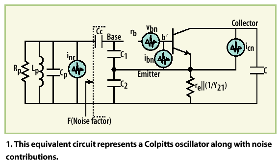
Equation 1 is limited by the fact that loaded Q typically must be estimated; the same applies to the noise factor. The following equations, based on this equivalent circuit, are the exact values for Psav, QL, and F, which are required for the Leeson equation. Figure 1 shows the typical simplified Colpitts oscillator giving some insights into the novel noise calculation approach.4
From ref. 3, the noise factor can be calculated by:
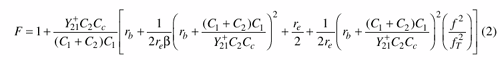
After some small approximation,
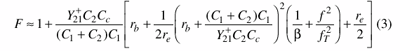
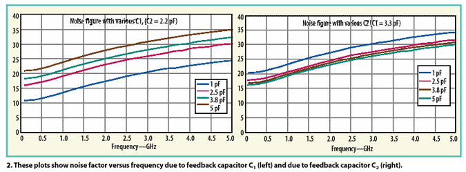
Figure 2 (left) illustrates the dependency of the noise factor on feedback capacitors C1 and C2. From Eq. 1, the phase noise of the oscillator circuit can be enhanced by optimizing the noise factor terms as given in Eq. 3 with respect to feedback capacitors C1 and C2.
Equation 4 can be found by substituting 1/re for Y21+ (+ sign denotes the large-signal Y-parameter).
When an isolating amplifier is added, the noise of an LC oscillator is determined by Eq. 5.
where:
G = the compressed power gain of the loop amplifier;
F = the noise factor of the loop amplifier;
k = Boltzmann's constant;
T = the temperature (in degrees K);
P0 = the carrier power level (in W) at the output of the
loop amplifier;
F0 = the carrier frequency (in Hz); fm = carrier
offset frequency (in Hz);
QL = (πF0τg) = the loaded Q
of the resonator in the feedback loop; and aR and aE =
the flicker noise constants for the resonator and loop amplifier, respectively.
From ref. 4, the output power for the Colpitts oscillator circuit of Fig. 1 can be calculated by:
where:
n = 1 + (C1/C2);
Vce = the collector-emitter voltage (< Vcc);
RL = the load resistance; and
QL = the loaded quality factor.
The factor of 1000 is needed since the result is expressed in dBm and a function of n and C1.
To calculate the loaded Q (QL), it is necessary to consider the unloaded Q (Q0) and the loading effect of the transistor. The influence of Y21+ must also be considered. The inverse is responsible for the loading and reduction of the Q.
Based on the transformation of the loading of the device emitter's differential impedance (resistance), it is possible to calculate the noise factor of the transistor under large-signal conditions. Considering the large-signal transconductance, Y21+,
which can be determined from the large-signal approach, this new approach to calculating the noise is based on existing general noise calculations. The approach applies to bipolar transistors but an equivalent procedure can be found for FETs.
Given an ideal resonator, with no long-term drift, aging, or variations due to temperature, tuning circuits would not be needed to correct for these performance shortcomings. But for practical applications, resonators require corrective measures to keep them on frequency. This is typically achieved through the use of tuning diodes with capacitance values that change as a function of applied voltage. In a Colpitts oscillator configuration with quartz crystal resonator, a capacitive voltage divider is used and the crystal acts like a high-Q inductor, slightly detuned from its series resonant condition. Since quartz crystal is a mechanical resonator driven by the piezoelectric effect, fundamental and a variety of overtone frequency modes (3rd, 5th, 7th, and 11th overtones) are possible. Unfortunately, undesired mode jumping is also possible even in well-planned circuit designs.
Circuitry must be added for a VCXO to remain in a desired operating mode. For example, if the fifth overtone mode is desired, a poorly designed oscillator may jump to the third overtone mode unexpectedly. Typically, crystal oscillators operate from about 1 to 150 MHz. Higher frequencies are possible, but the crystal resonators become thinner for higher-frequency operation and aging effects increase.
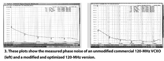
To demonstrate the new VCXO optimization approach, a commercial 120-MHz VCXO was used as an example to apply the concept of conduction angle as outlined earlier.4 Figure 3 shows the typical measured phase noise of the VCXO before (left) and after (right) the first modification, respectively.
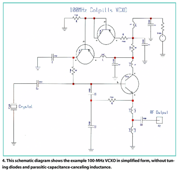
As another example, a 100-MHz crystal-controlled Colpitts oscillator was designed according to a set of specifications that included +13 dBm output power, 50-Ω load, and phase noise of –132 dBc/Hz offset 100 Hz from the carrier, with the intention of applying the new approach to this basic design to achieve improved performance (Fig. 4).
The first step in the design process involved calculating the operating point for a fixed normalized drive of x = 20 (Table 6-1 in ref. 3). The output voltage at the fundamental frequency, based on the output-power requirement, can be found from Eq. 8.
![]()
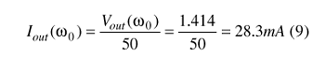
The fundamental current can be found from Eq. 9.
The DC operating point is calculated based on the normalized drive level x = 20. The expression for the emitter DC current can be given in terms of the Bessel function with respect to the drive level can be found with Eq. 10.
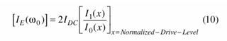
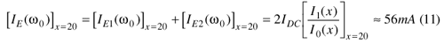
For the normalized drive level x = 20, the output emitter current at the fundamental frequency can be given as Eqs. 11 and 12.
![]()
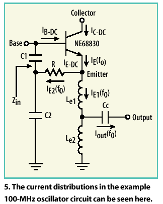
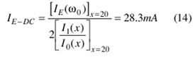
Figure 5 shows the oscillator circuit configuration with DC and RF current distribution components as describes in Eqs. 13 and 14.
![]()
For this typical example, an NE68830 transistor from NEC was selected for validation.
The second step in the design process involved the development of the biasing circuit. For the best close-in phase noise, a DC/AC feedback circuit is incorporated to provide the desired operating DC conditions,3 with IE = 28.3 mA, VCE = 5.5 V, supply voltage, Vcc = 8 V, = 120, and IB ≈ 0.23 mA.
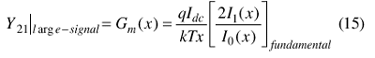
The third step involves calculating the large-signal transconductance (see Tables 6-1 and 6-2 in ref. 3) using Eqs. 15 and 16.
![]()
The fourth step in the procedure involves the calculation of loop gain, which can be found from Eqs. 17 and 18.
![]()
![]()
where Rp1(f0) is the equivalent resistive load across the port 1 (Fig. 6).
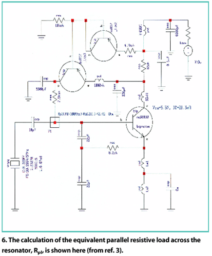
For practical purpose, the loop gain should be 2.1 to achieve good starting conditions for oscillation.
From Eq. 10, it is possible to derive Eq. 19.
![]()
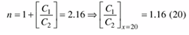
The fifth step in the design procedure involves calculation of the feedback capacitor ratio by means of Eq. 20.
The next step involves calculation of the absolute value of the feedback capacitor by means of Eq. 21. In this case, Zin (looking into the base of the transistor) can be calculated by means of Eq. 21.3

where:
CP = (CBEPKG + Contribution from layout) = 1.1 pF and
LP = (LB + LBX + the contribution
from layout) = 2.2 nH.
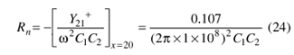
The expression for the negative resistance (Rn, without parasitics) is found by means of Eqs. 22-24.
![]()
![]()
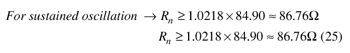
For sustained oscillation, the conditions are shown in Eq. 25.
From Eqs. 17 and 18, it is possible to derive Eq. 26.

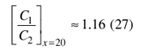
From Eq. 13, it is possible to derive
Eqs. 27 and 28.
![]()
where C2 = 22 pF and, for practical purposes, C1* = 22 pF.
The final step in the approach involves calculating the phase noise. From Eqs. 1 through 6, the calculated phase noise offset 100 Hz from the carrier, using the modified Leeson equation, is –132 dBc/Hz. Simulated results (not shown here) and calculated data for the example 100-MHz oscillator, along with the measurements, agree within about 2 dB.
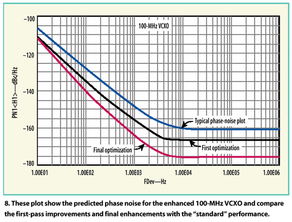
By applying the patented technology,5-8 Fig. 7 shows the resulting simplified schematic diagram for an enhanced-performance 100-MHz VCXO. Figure 8 shows a phase-noise plot for the improved 100-MHz oscillator after applying noise filtering, controlled RF conduction angle, and delay feedback as outlined in the patents.5-8 The new approach can be used to improve the performance of inexpensive low-Q crystal resonators for cost-effective signal generation.
Figure 8 also compares the simulated "off-the-shelf" phase noise of the VCXO with a first-pass optimization and with the best results from these new techniques. The simulated results from Ansoft Designer were validated with theory and measurements.3 Alternative VCXO topologies can not compete with these results in terms of cost, size, power, phase noise, and reconfigurability. The new approach includes evanescent-mode coupling for optimum group delay to enhance the loaded Q and suppress mode-jumping phenomena (especially when the crystal resonates at higher odd-order overtone modes). It also minimizes the effects of thermal drift without sacrificing phase-noise performance.8
The approach shown at 100 MHz is being applied in the development of high-performance VCXOs to be used in Synergy Microwave's lines of advanced frequency synthesizers. The technique can also be extended to higher frequencies by incorporating mode-injection stubs across the crystal resonator for the desired operating frequency. The technique is available for licensing; interested parties are advised to contact one of the authors.