The phenomenon of phase noise generation in oscillator/VCOs has been the main focus of important research efforts and is still an open issue, despite significant gains in practical experience and modern CAD tools for design. In the design of oscillator/VCOs, minimization of the phase noise is the prime task and this objective has been accomplished using empirical rules. Therefore, the predictive power of the model is limited.1–5 The phase noise is a critical figure-of-merit because it affects the dynamic range, selectivity and sensitivity of a receiver.2–4 The ability to achieve minimum phase noise performance is paramount in most RF and MW designs, and the continued minimization of phase noise in oscillator/ VCOs is required for the efficient use of the frequency spectrum. This article presents an analytical approach for noise minimization techniques in terms of the oscillator circuit component parameters, leading to minimum phase noise for a given class of VCO topology.5–27
Oscillator Theory
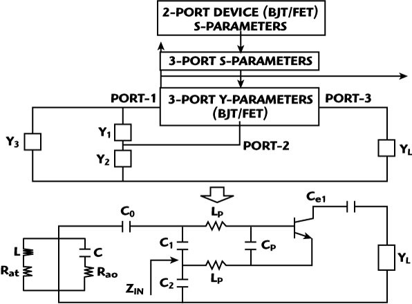
Fig. 1 Colpitts oscillator with base lead inductance and package capacitance using a three-terminal active device.
Figure 1 shows a simplified Y matrix approach to describe a typical oscillator circuit and the flow chart on how to convert two-port S-parameters to a three-port configuration, using a three-terminal active device. The expression for the input impedance of the oscillator circuit shown is given by
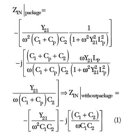
where
Yij (i,j=1,2) = Y-parameters
Lp = base-lead inductance
Cp = base-emitter package capacitance of the BJT
From Equations 1 and 2, the base-lead inductance makes the input capacitance appear larger and the negative resistance appears smaller. The equivalent negative resistance RNEQ and capacitance CEQ can be defined as4
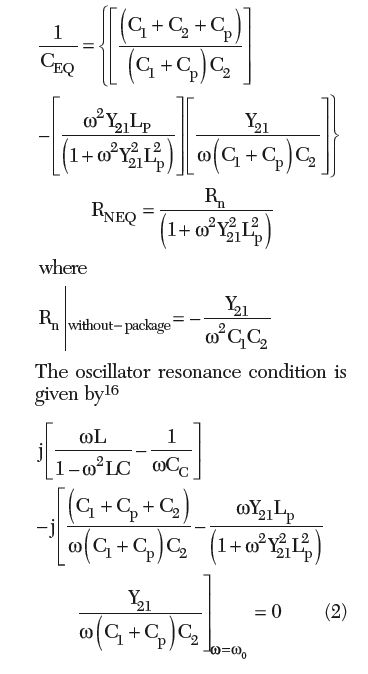
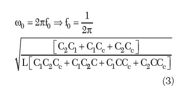
where
f0 = oscillator resonance frequency
The performance of an oscillator can be evaluated by the figure-of-merit (FOM) and can be described by
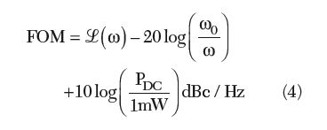
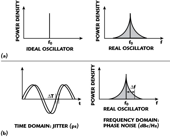
Fig. 2 Frequency spectrum of ideal and real oscillators (a) and jitter in time domain relating to phase noise in the frequency domain (b).
The first and third terms of Equation 11 represent the contributions of phase noise and power consumption (PDC) to FOM, respectively. From Equation 11, the phase noise for a given offset has a greater impact on FOM than the power consumption does for a given oscillator frequency f0. From Equation 3, the degree to which an oscillator generates a constant frequency f0 throughout a specified period of time is defined as the frequency stability of the signal source. The frequency instability, due to the presence of the noise in the oscillator circuit, modulates the signal, causing a change in frequency spectrum commonly known as phase noise. Figure 2 illustrates the frequency spectra of ideal and real oscillators and the frequency fluctuation corresponding to jitter in the time domain, which is a random perturbation of the zero crossing of a periodic signal.
Phase noise and timing jitter are both measures of uncertainty in the output of an oscillator. Phase noise defines the frequency domain uncertainty of an oscillator, whereas timing jitter is a measure of oscillator uncertainty in the time domain. The equation for an ideal and real oscillator in the time domain is given by4


where A0, A(t), φ0, φ(t) and f0 are the fixed amplitude, time variable-amplitude, fixed phase, time variable-phase and free running frequency of the oscillator.
From Equations 5 and 6, the fluctuations introduced by A(t) and φ(t) are functions of time and lead to sidebands around the center frequency f0, giving a direct relationship between phase noise and the spectral output of the oscillator. The phase noise is defined in terms of the noise spectral density, in unit of decibels below the carrier per Hertz and is given by
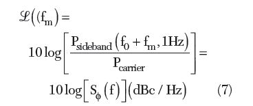
From Equation 7, the expression for the phase noise is given by16
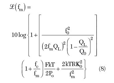
where ![]() (fm), fm, f0, fc, QL, Q0, F, k, T, Po, R and K0 are the ratio of the sideband power in a 1 Hz bandwidth at fm to total power in dB, offset frequency, flicker corner frequency, loaded Q, unloaded Q, noise factor, Boltzman’s constant, temperature in Kelvins, average output power, equivalent noise resistance of tuning diode and voltage gain.
(fm), fm, f0, fc, QL, Q0, F, k, T, Po, R and K0 are the ratio of the sideband power in a 1 Hz bandwidth at fm to total power in dB, offset frequency, flicker corner frequency, loaded Q, unloaded Q, noise factor, Boltzman’s constant, temperature in Kelvins, average output power, equivalent noise resistance of tuning diode and voltage gain.
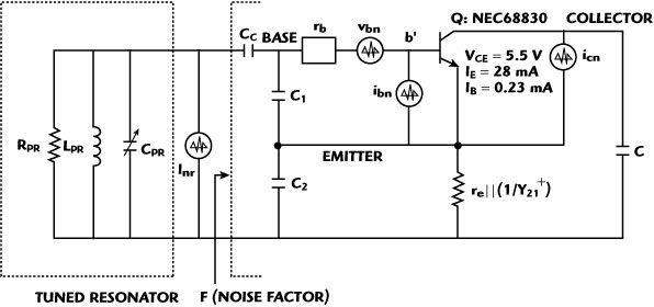
Fig. 3 Equivalent circuit of a Colpitts oscillator with noise sources.
From Equation 8, the phase noise performance depends on the noise factor F of the oscillator circuit for a given resonator network and oscillator/VCO topology; therefore, optimization of the noise factor will lead to the minimization of the phase noise. Figure 3 shows the equivalent circuit of a Colpitts oscillator for the purpose of the noise factor analysis.4,16 The predictive power of Equation 8 is limited due to the parameter noise factor F, which is not known a priori. The approximate expression of the noise factor F in terms of the oscillator feedback components (C1 and C2) for the circuit shown is given by4

From Equations 3 and 4, the free running frequency f0 of the oscillator circuit is given by4
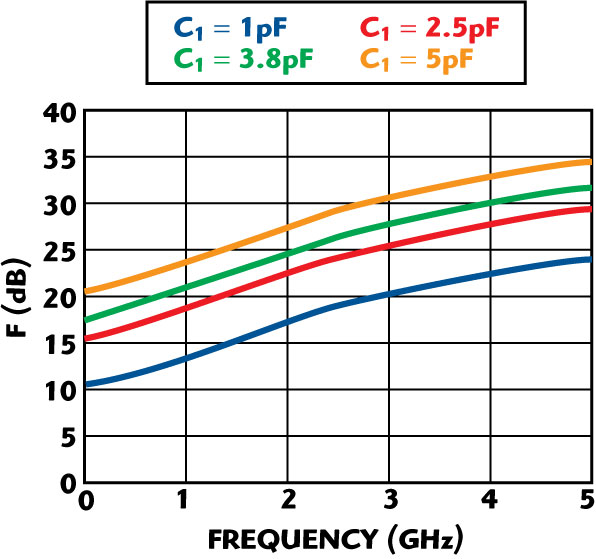
Fig. 4 Noise figure vs. frequency as a function of C1 with C2 = 2.2 pF.
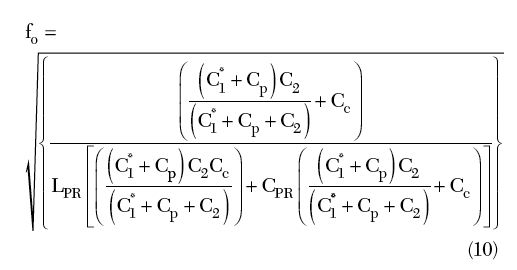
With the transistor (Q) NEC68830, C = 2.2 pF, CP = 1.1 pF, C1 = C
 + CP = 3.3 pF, C2 = 2.2 pF, Cc = 0.4 pF, RPR = 18000, CPR = 4.7 pF, LPR = 5 nH; the free running frequency is calculated from Equation 10 as f0
 1000 MHz.
With Y = 0.002 (large-signal Y-parameter), re = 0.9 Ω at 28 mA, ß = 100, f = 1 GHz, fT = 10 GHz; the noise factor F is calculated from Equation 6, as F = 104.7
  NF = log10(F) = 20.18 dB.
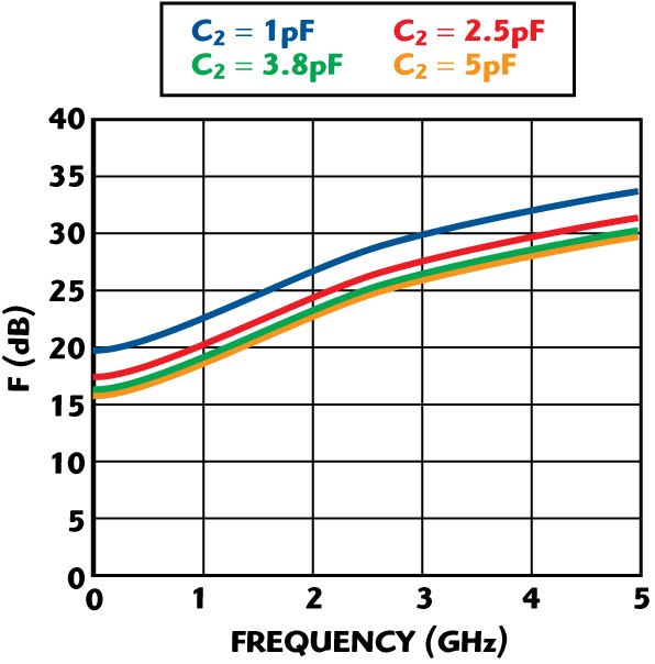
Fig. 5 Noise figure vs. frequency as a function of C2 with C1 = 3.3 pF.
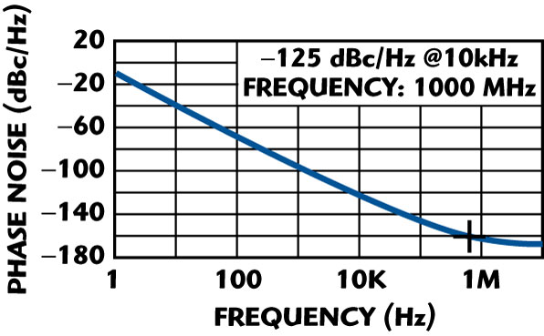
Figures 4 and 5 illustrate the dependency of the noise figure F (dB) on feedback capacitors C1 and C1. From Equation 8, the phase noise of the oscillator circuit can be optimized by optimizing the noise factor terms as given in Equation 9, with respect to the feedback capacitors C1 and C2. For the example circuit shown, the output power = 13 dBm, C1 = 3.3 pF, C2 = 2.2 pF, Y
With Y = 2 mS, Q0 = 1000, QL = 380, F = 20 dB (calculated from Equation 9). From Equations 8, 9 and 10, the calculated phase noise plot for the circuit is shown in Figure 6, which closely agrees with the simulated (Ansoft Designer) phase noise plot within the variation of 3 dB, as shown in Figure 7.
From Equation 8,

where
m = ratio between the loaded and unloaded Qs
From Equations 8 and 11, the minimum phase noise can be found by differentiating Equation 11 with respect to m, and equating to zero for maxima and minima as4
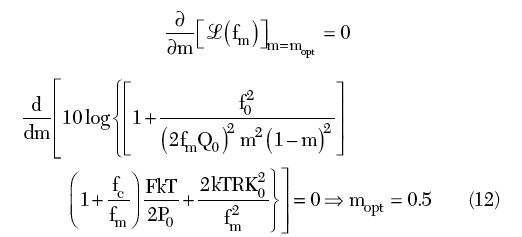
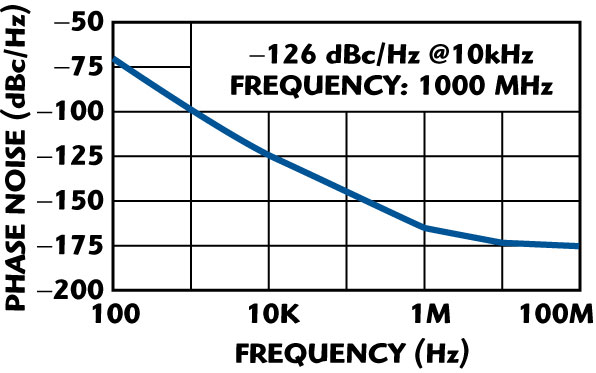
Figure 8 shows the typical phase noise plot at 10 kHz offset with respect to m for the 1 GHz oscillator circuit. For different values of the noise figure F (F3 > F2 > F1), the phase noise is minimum at mopt, and the plot is typically like a bathtub curve, which is shifted symmetrically about mopt.
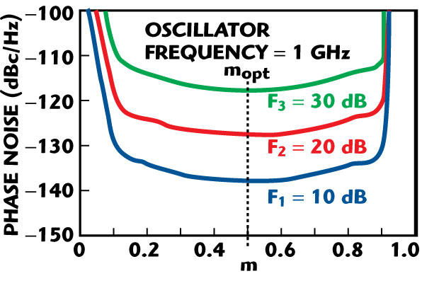
Fig. 8 Phase noise vs. m at 10 kHz offset for different values of F.
This implies that for low noise wideband application, the value of m should be dynamically controlled over the tuning range and should lie in the vicinity of mopt for minimum phase noise performance.14–26
From Equation 9, the circuit topology and the resonator are selected in such a way that the feedback parameters (C1 and C2) are dynamically tuned for minimum noise figure (F), and m = 0.5 over the desired tuning range. From Equation 8, the phase noise of the oscillator circuit can be described exclusively in terms of the prior known circuit parameters as16
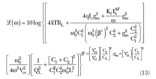
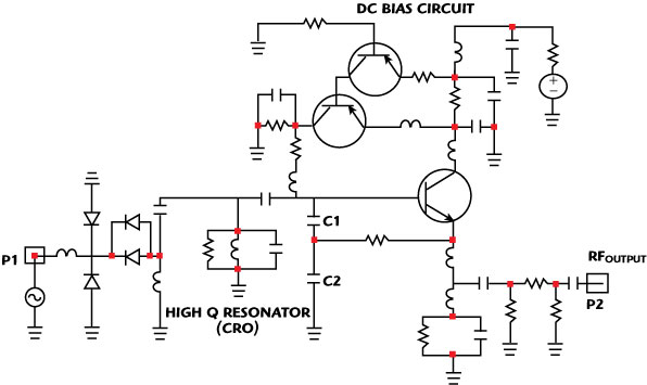
where y+21, y+11 are the large-signal [Y] parameters of the active device, Kf is the flicker noise coefficient, AF is the flicker noise exponent, RL is the equivalent loss resistance of the tuned resonator circuit, Ic is the RF collector current, Ib is the RF base current, Vcc is the RF collector voltage, C1, C2 are the feedback capacitors, and p and q are constants depending upon the drive level across the base-emitter of the device.16 To test the validity of the noise models, a 1 GHz Colpitts VCO was built, which is shown in Figure 9. Figure 10 shows the measured plot of the phase noise, which is in good agreement within 2 to 3 dB with the calculated and simulated results shown previously.
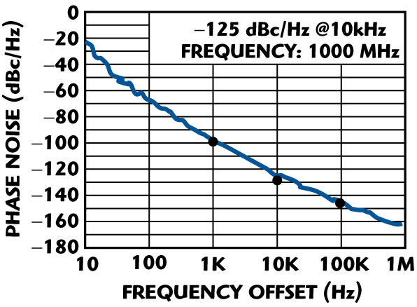
Fig. 10 Measured phase noise of the fabricated VCO.
Noise Impedance Matching
Minimizing of the noise level can be done by a noise impedance matching analog to power matching by means of a transformer. For high frequency oscillation, noise impedance matching using a transformer winding is practically limited. The other alternative is to match the impedance by incorporating a capacitive tapping factor n of the resonator network for optimum noise impedance level. Here, the tapping factor n is analogous with the conventional transformer-winding ratio. Figure 11 shows the equivalent representation of a capacitively tapped series resonator network. As shown, capacitive tapping increases the impedance level at the terminals of the resonator network, which is required for the impedance matching for minimum noise factor, thereby improving the phase noise performance. However, the tapping mechanism introduces an additional parallel capacitance, Cresonator and Ctap, which yields an unwanted mode of oscillation.

Fig. 11 Equivalent representation of a capacitively tapped series resonator.
Care must be taken to avoid the unwanted parasitic mode of oscillations, which otherwise degrades the loaded quality factor of the resonator when the parallel parasitic resonance is relatively close to the fundamental series resonance. The fundamental resonance frequency and transformed resonator impedance can be described by

where
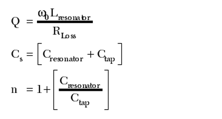
From Equation 15, the transformed resonator impedance [Z(ω0)] depends upon the tapping factor n, and can be optimized for maximum signal-to-noise ratio to minimize the phase noise. Due to the tapping


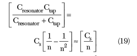
From Equation 19, as the tapping factor n increases, the parallel unwanted parasitic resonance mode tends to shift towards the fundamental series resonance mode. The effective quality factor Q of the resonator decreases due to the tapping for noise impedance matching,4 and can be described by
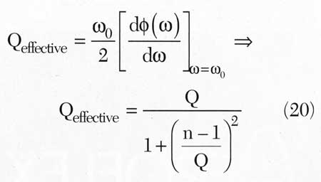
From Equation 20, when the tapping factor n is small, the degradation of the quality factor is negligible. The parasitic mode of the frequency can be given by
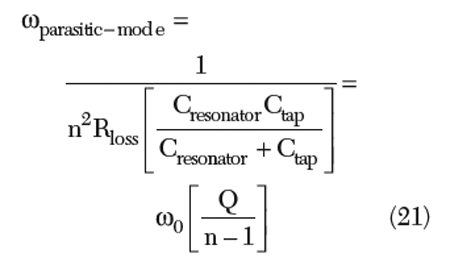
To prevent the unwanted parasitic mode of resonance, the tapped resonator should be compensated by the negative resistance and the negative capacitance. The negative resistance will compensate the loss resistance n2Rloss, and the negative capacitance cancels the effect of the positive the Cresonator and Ctap. By proper selection of an optimum tapping factor nopt, which depends on the loss resistance of the resonator and the active device (BJT/FET) parameters (especially the base resistance of the bipolar transistor), the noise impedance matching can be done for improved phase noise performance.
An oscillator circuit can support more than one resonant mode (unwanted parasitic oscillations due to the bonding wire inductance Lp), which can be described by the admittance equation as
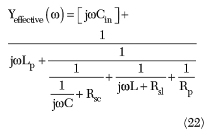
From Equation 22, the fundamental parallel mode of oscillation is given by the parallel combination of L and [1/jω (Cin+C)], but there is a second parasitic mode associated with [1/jωCin] in parallel with [jωLp+ jωL] and [1/jωC], which is due to the parasitic bonding wire inductance Lp. The parasitic oscillation mode can be overcome by incorporating a resistor Rs to Lb, which will damp the spurious parasitic oscillation mode and has negligible effect on the fundamental resonance mode. However, care needs to be taken in the design, since a large value of Rs increases the noise factor, thereby degrading the overall noise performance of the Colpitts oscillator circuits.
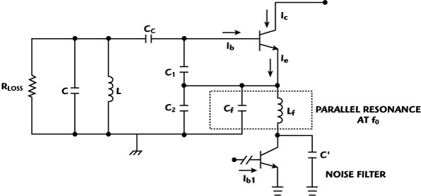
Fig. 12 Typical Colpitts oscillator circuit with a noise filtering network.
Noise Filtering
Figure 12 shows the noise-filtering network at the emitter bias current (Ie) in a typical Colpitts oscillator circuit. The feedback capacitor C2 should remain unaffected by the insertion of the filter, which means that an additional capacitance Cf may be required to cancel the inductor reactance Lf at the fundamental oscillation frequency. The single-ended bipolar transistor circuit in which filter inductor Lf tunes the parasitic capacitance to the oscillation frequency can serve this purpose. Simulation CAD and measured data confirm the improvement by 3 to 6 dB of the phase noise.14
Optimum Transconductance (gm)
There are mainly two noise sources that mostly contribute to the phase noise: thermal noise (broadband noise) and flicker noise (low frequency noise). Flicker noise up-conversion is related to the symmetry of a signal waveform and can be reduced by designing the signal swings symmetrically.
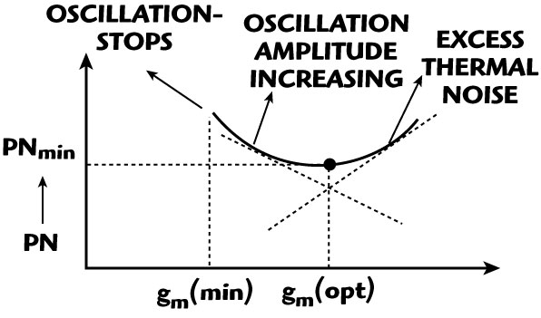 Fig. 13 Typical plot of phase noise vs. transconductance.
The active device in the oscillator circuit generates the negative conductance to compensate for the loss in the resonator network in order to sustain a steady-state oscillation, thereby generating a broadband thermal noise proportional to the negative transconductance of the device. If the negative transconductance is very small, then it does not support steady-state oscillation, whereas, if it is very large, it generates an excess thermal noise that may increase the oscillator phase noise drastically. Therefore, the transconductance of the device should be optimized in order to maintain stable oscillation without introducing excessive noise. Figure 13 shows a typical plot of the phase noise versus device transconductance. The oscillator starts oscillating when the transconductance reaches gm(min) and it is just sufficient enough to compensate the loss in the resonator tank. As the transconductance increases from gm(min), the phase noise decreases till it reaches gm(opt). Any further increase in transconductance creates a counter effect and the thermal noise in the active device increases and follows the transconductance curve. Therefore, corresponding to gm(opt), the phase noise reaches the minimum point and, after that, the increase in oscillation amplitude is completely nullified by the increase in thermal noise. After crossing the minimum point, the phase noise increases as the signal amplitude is limited to the supply voltage, while the thermal noise continuously increases with the increase in conductance. Therefore, for a given oscillator topology, there exists an optimum transconductance for the minimum phase noise.
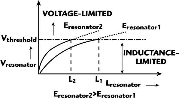 Fig. 14 Two zones: Voltage limited and inductance limited.
Optimum Inductance (L)
As shown in Figure 14, two modes of operation exist for an LC oscillator, namely current and voltage regimes. Considering the bias current as an independent variable, the voltage across the resonator network can be described by


In the current-limited zone, the resonator tank amplitude Vresonator linearly increases the bias current according to the relationship, until the oscillator enters the voltage-limited zone, whereas, in the voltage-limited zone, the amplitude is limited to the Vthreshold, which can be determined by the available supply voltage.
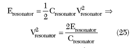


The equivalence of the current and inductance-limited zone can be combined to determine the relation between Eresonator and Ibias in the inductance-limited zone.


The noise-to-carrier ratio can be given as
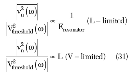
From Equation 31, the noise-to-carrier ratio remains constant in the L-limited zone and does not depend on the value of the inductor. However, once the oscillator enters the voltage limited zone, the noise-to-carrier ratio increases with L. Therefore, selecting an L, which transfers the oscillator in the voltage-limited zone, yields a waste of L and increases the noise. For a given energy Eresonator, a larger Vresonator obtained by increasing the L does not offer a better noise performance since the oscillator has a similar response to both the Eresonator and the thermal energy.
Self-injection Mechanism
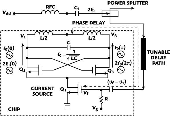 Fig. 15 Self-injected coupled oscillator.
Minimizing of the noise can be done by employing a self-injection locking mechanism in a coupled oscillator, which is a cost-effective and power-efficient alternative and has recently emerged as a strong contender for low noise signal sources in modern wireless communication systems.2–4 Figure 15 shows the second-harmonic self-injected coupled oscillator topology, which consists of a cross-coupled pair (Q2–Q3), a current source (Q1), a power splitter, and a tunable delay path containing a delay-line cable and a tunable phase shifter.27 Figure 16 shows the simplified oscillator model consisting of an LC tank, a conductance (Gt) representing the tank loss, a feedback signal Vf(t) and the mildly nonlinear transconductance (gm1 to gm3). For the self-injected coupled oscillator, part of the output signal feeds back to the current source. The current source with the mildly nonlinear transconductance (gm1) transforms the feedback signal Vf(t) to a larger current format [If(t) = gm1Vf(t)]. With the equivalent parallel resistance of the tank Req for the second-harmonic (2f0), the feedback signal amplitude crossing the tank (Vinj) is produced [Vinj(t) = If(t).Req]. The expression of the phase fluctuation (phase noise) of the self-injected coupled oscillator is27
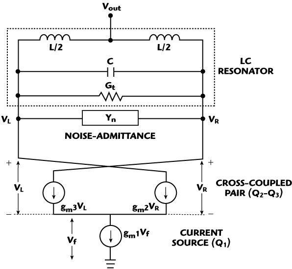 Fig. 16 Simplified model of the self-injected coupled oscillator.
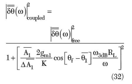
For (θf–θ1) ⇒ 2nπ Equation 32 can be given by
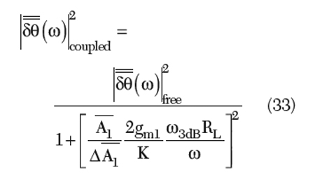
From Equation 33, the noise can be further minimized by increasing the transconductance (gm1) of the current source, increasing the equivalent parallel-resistance of the tank (RL) for the fundamental signal (f0), reducing the amplitude imbalance (Δ![]() ) for the second-harmonic signal and increasing the second-harmonic amplitude (
) for the second-harmonic signal and increasing the second-harmonic amplitude (![]() ).
).
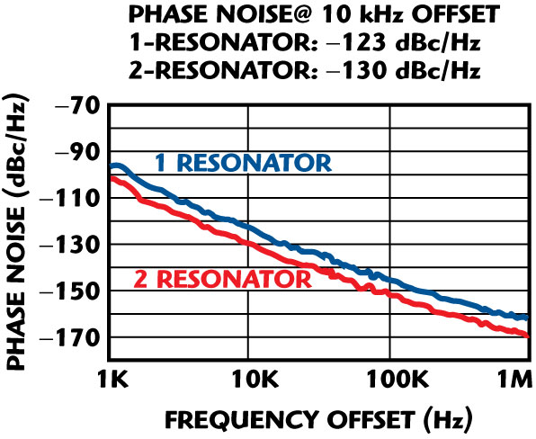
Fig. 17 Measured phase noise plots of 2488 MHz oscillators using a CPR configuration (two resonators) and uncoupled resonator oscillator (one resonator).
Examples: Low Noise Oscillators
Coupled Planar Resonator-based 2488 MHz Oscillator
The following example describes the use of coupled planar resonator (CPR) and noise minimization techniques as discussed in the previous section for a high performance, low noise, high quality microwave source. A CPR-based 2488 MHz VCO was designed and fabricated on a 0.35" x 0.35" x 0.16" substrate and experimental results have validated the novel techniques proposed in this work. Figure 17 shows the phase noise plot of the 2488 MHz VCO using CPR resonators in a hybrid medium (transverse coupling between stripline and microstrip line coupled resonators, PCB: six-layer board with Rogers substrate) and the operating bias conditions are Vcc = 5 V, Ic = 15 mA. The measured phase noise plot of the oscillator minimizes the noise and shows a 7 dB reduction in phase noise, with respect to the uncoupled planar resonator-based oscillator with a typical power output of 5 dBm (minimum) and 30 dB harmonic rejections.
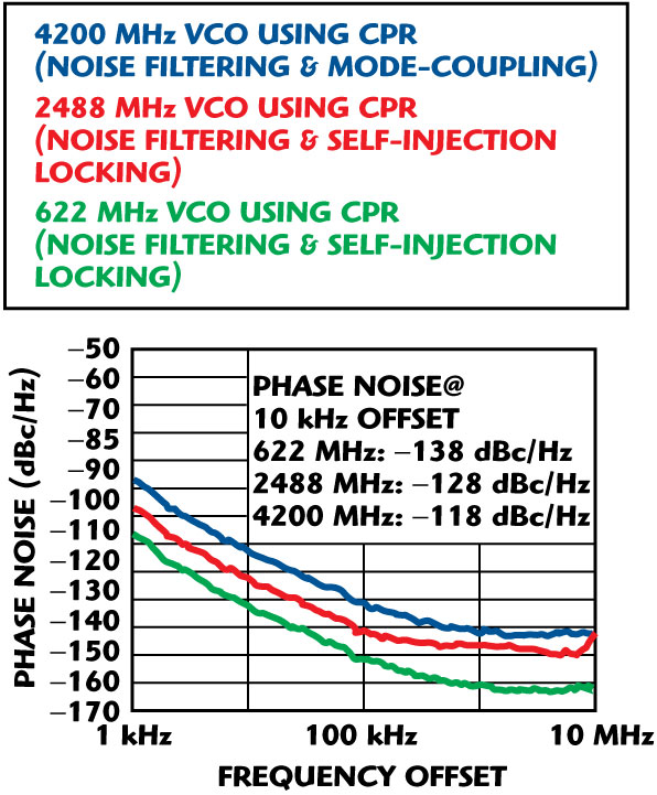
Fig. 18 Measured phase noise of 622/2488/4200 MHz VCOs using CPR.
For the validation of the approach, 622, 2488 and 4200 MHz VCOs were designed and fabricated, where the resonator is self-injection locked and tuned to their respective fundamental frequencies (without frequency multiplication). Figure 18 shows the phase noise plot for comparative analysis of 622, 2488 and 4200 MHz VCOs using CPR and noise reduction techniques.
Power Efficient and Low Microphonics VCOs
An object of this research work is to provide a cost-effective solution to solve the problem of microphonics and conversion efficiency by using stubs tuned planar-coupled resonators (STPCR) in a stripline medium (since they are self-shielding due to their dual ground plane) for low noise signal sources, which can replace a low power oscillator followed by an amplifier, in order to reduce the size and cost of the wireless communication systems.3,14,15,19 DC-to-RF conversion efficiency is related to the fundamental signal RF output power and DC power consumption, which can be described by
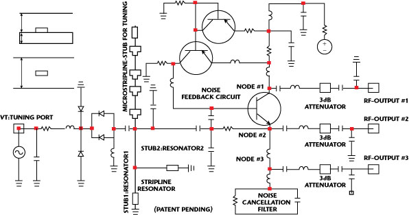 Fig. 19 Schematic of a self-coupled, shorted-stubs resonator oscillator (patented).
where
ηefficiency = DC-to-RF conversion efficiency
P(ω0) = RF output power of the fundamental signal
PDC = DC power consumption
For higher conversion efficiency, the oscillator circuit topology should be such that it operates at low DC power and at the same time produces high RF output power at the desired fundamental frequency. The RF output power for a typical oscillator circuit can be described in terms of the higher order harmonics as
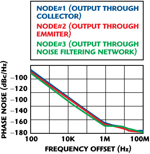 Fig. 20 Simulated phase noise of the self-coupled, shorted-stubs resonator oscillator.
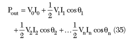
where V1, I1, V2 I2 and Vn, In are the amplitudes of the voltage and currents of the fundamental, second and nth harmonic components, respectively; the angles θ1, θ2 and θn are the phase angles between the voltage and the current of the respective harmonic components present at the output node of the oscillator circuit. For a high value of ηefficiency, other higher order harmonics must be suppressed; otherwise, they will degrade the conversion efficiency of the generated fundamental signal tone (ω0) from the given input DC power (VDC x IDC).
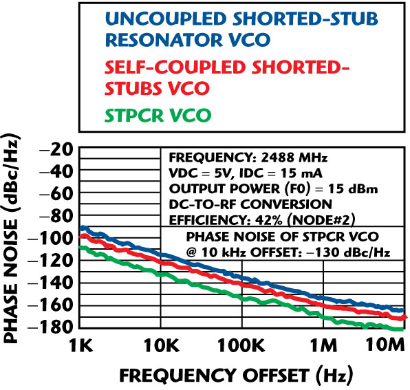 Fig. 21 Measured phase noise of the STPCR VCO.
Figure 19 shows the schematic of a typical 2488 MHz STPCR oscillator circuit, where the RF output is extracted from three different nodes (Nodes 1, 2 and 3) for comparative analysis of the DC-to-RF conversion efficiency and phase noise performances. Figure 20 shows the simulated (CAD: Ansoft Designer Nexxim V3) phase noise plot for the oscillator circuit, which shows that the RF output extracted through Node 3 ultimately offers the best phase noise performance. As depicted, Node 3 gives a higher level of second-order harmonic rejections (45 dB) in comparison to Node 2 (30 dB) and Node 1 (15 dB). However, Node 2 offers higher efficiency (40 percent) in comparison to Node 1 (10 percent) and Node 3 (20 percent); therefore, there is trade-off between phase noise and harmonic rejection based on the applications.
Figure 21 shows the phase noise plot of the STPCR-based, high spectral pure signal source at 2488 MHz in accordance with the present novel techniques (patent-pending), which can be tuned (user-defined frequency) and where the frequency can be extended without changing the dimensions of the stub-tuned resonators (stripline domain PCB: six-layer). The design is based on an innovative topology, which supports the fast convergence by dynamically tuning the noise impedance transfer function of the resonating network and the negative resistance generating device for optimum noise performance over the tuning range. The measured phase noise for a 2488 MHz carrier frequency is typically –128 dBc/Hz at 10 kHz offset from the carrier with 40 percent DC-to-RF conversion efficiency. The measured RF output power at the fundamental frequency f0 is typically 15 dBm for a given operating DC bias condition (VDC = 5 V, IDC = 15 mA).
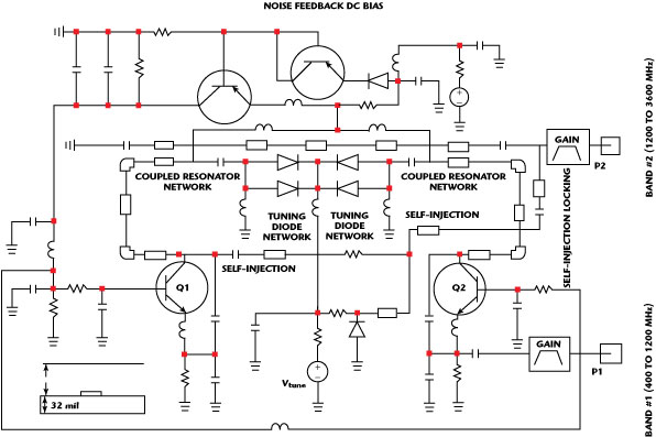 Fig. 22 Schematic of a coupled oscillator self-injection locked VCO.
Coupled Oscillators Self-injection Locked Wideband VCO
Figure 22 shows the schematic of the configurable signal source by using the coupled oscillator self-injection locked mechanism and noise reduction techniques discussed previously. The circuit works at 5 V and 32 mA and the tuning voltage is 0 to 28 V. The typical RF output power is 5 dBm over the tuning range and sub-harmonic rejection is better than 20 dB. Figure 23 shows the measured phase noise plot of the configurable signal source, which is better than –105 dBc/Hz at 10 kHz offset from the carrier for the frequency band.
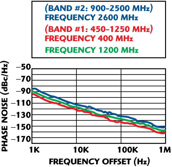 Fig. 23 Phase noise of the dual-band coupled oscillator self-injection locked VCO.
Active Resonator (AR)-based Low Noise Oscillator
Normally, in the AR topology, the CPR is coupled to the negative resistance generating device network so that, in principle, an AR element similar to the general oscillator is being created. A general oscillator needs both the amplitude and phase conditions to be satisfied for oscillation build up at f0. In the case of the AR, only the phase condition for oscillation build up at f0 is required for stable and sustained oscillations and no amplitude condition is required to compensate for the loss of the AR from the active device network.28 As shown in Figure 24, the oscillations will not build up in AR and growth is restricted; therefore, an active amplifier can work in the small-signal linear regime. The gain and power of the amplifier added to the circuit will compensate the inner losses of the AR circuits, and full compensation (–|Gn| + G = 0) of W (energy losses) will result in infinite unloaded Q and improved loaded Q when coupled to a transmission line or equivalent oscillator circuit. AR based on a negative resistance approach offers improved Q factors, but they have drawbacks: the schematic is complex and must have a feedback element and matching networks to produce the negative conductance |–Gn|, sensitive to spurious oscillation (if the oscillation start-up condition is satisfied).
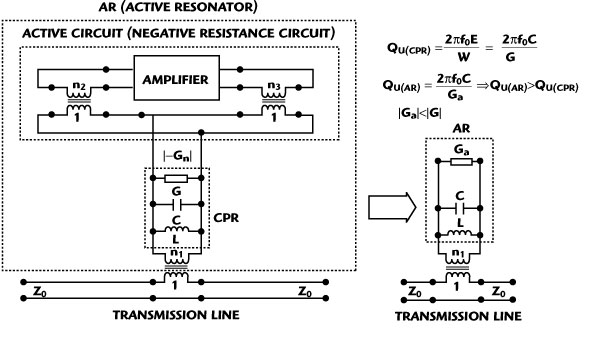 Fig. 24 Active resonator with feedback arrangement.
A normal oscillator requires the amplitude and phase condition to be satisfied for guaranteed and sustained oscillation build up at the desired frequency, whereas, for an active resonator element, only the phase condition needs to be satisfied. Hence, the oscillation will not build up across the active resonator and, therefore, the active resonator module can work in the small-signal regime (instead of the large-signal regime condition required for sustained and guaranteed oscillations). Moreover, the negative resistance, added to the active resonator circuit, will reduce the intrinsic losses of the passive resonators used as active resonators. This approach yields high Q resonators; however, active resonator elements are sensitive to spurious oscillations that may cause an unwanted oscillation mode in the event of satisfying the start-up oscillation condition. Since the conventional planar microstripline resonator itself is a lossy element, the unloaded Q factor is low and finite. Moreover, coupling the planar resonator to the external circuits (oscillator, filter, diplexer, etc.) results in loosing a finite amount of energy due to the coupling and other mechanism, thereby resulting in further degradation in the loaded Q factor. In addition, the excitation of other higher order oscillation modes across the resonators increases the resistive loss, which has to be compensated by the active resonator topology for low phase noise performance.
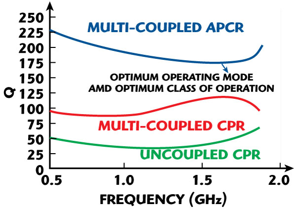 Fig. 25 Measured Q of planar resonators.
Figure 25 illustrates the measured Q of the typical planar-coupled resonators (uncoupled, coupled, ACPR) for the purpose of comparative analysis. Figure 26 shows the block diagram of an APCR (active planar-coupled resonator) VCO, which is based on a novel topology that supports minimum phase hits and broadband tunability, to compensating for the frequency drift due to temperature and aging, in a compact size and also amenable for integration in current IC technology. To overcome these problems, the active resonator is realized by incorporating an injection mechanism based on a feedback approach that can be dynamically controlled over the desired frequency band. By adjusting the feedback factor of the negative resistance generating circuit, the optimum value of the negative resistance to compensate for the loss of the CPR can be achieved. In this way, the conduction angle, the injection level and the group delay can be optimized towards the steepest phase characteristic curve for a given resonance condition across the active resonators. This condition leads to the operation of the APCR oscillator circuit in the vicinity of the evanescent domain. Hence, an improved group delay and phase characteristic curve are obtained, thereby increasing the effective dynamic loaded Q by many folds, resulting to low phase noise.
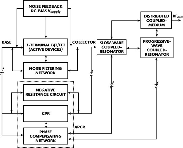 Fig. 26 Block diagram of the APCR VCO (patent pending).
The layout of the APCR VCO is a six-layer board, fabricated on a 64 mil thick Rogers substrate of dielectric constant 3.38 and loss tangent 2.7(10–4). The choice of substrate depends on size, higher order modes, surface wave effects, implementations (couplings, line length, width, spacing and spacing tolerances), dielectric loss, temperature stability and power handling (dielectric strength and thermal conductivity). The APCR circuit works at 5 V and 25 mA, with an output power of 2 dBm, and second-harmonic rejection is better than -20 dBc. Unfortunately, each development design of a VCO, using APCR technology, has its price, since they occupy larger PCB area and, for the same space, exhibit much lower Qs compared to a high Q, CRO/SAW resonator. For the most part, these disadvantages have been overcome by means of a mode coupling approach, which acts as a Q-multiplier, and minimization of noise over the band is achieved by incorporating a noise-filtering network, a noise cancellation network, a phase compensating network and a noise feedback bias circuit.16 Figure 27 shows the measured phase noise plot of the APCR VCOs at 2560 MHz with a 1 percent tuning range. Figure 28 shows the temperature and frequency drift profile of commercially available CROs and the new APCR VCOs (this work) for the purpose of the comparative analysis about the thermal drift profile and frequency tuning range (Δf). As depicted, the APCR VCO offers broadband tunability, extended operating temperature range and overcome the limiting performance of the frequency drift due to temperature and component tolerances.
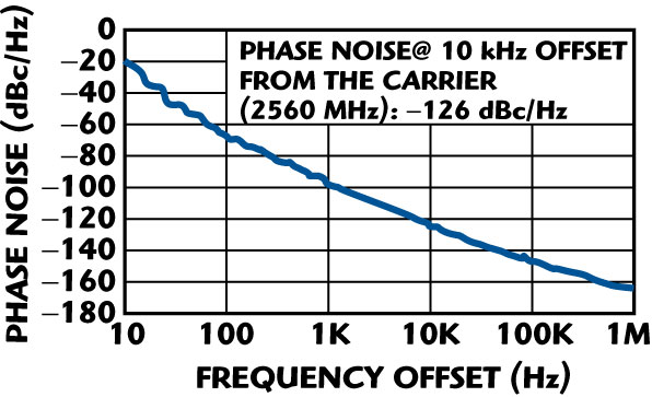 Fig. 27 Measured phase noise of an APCR VCO at 2560 MHz.
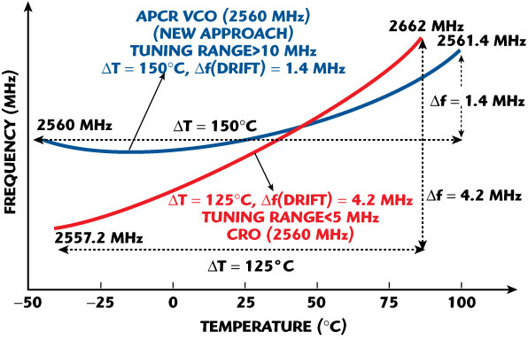
Fig. 28 Measured thermal drift and frequency tuning range of commercially available CROs and the new APCR VCO.
Conclusion
With regard to the state-of-the-art of the configurable signal source, this novel approach provides a general concept of reducing the noise over the frequency bands; it can help to avoid pitfalls that can increase the time required to achieve minimum phase noise over the band, and offers a promising alternative for high Q planar resonators in the context of a planar fabrication process, compatible with existing IC and MMIC processes.